
Data Sheet

Final Datasheet
BME280 Environmental sensor
Page 35
BST-BME280-DS001-10 | Revision 1.1 | May 2015 Bosch Sensortec
© Bosch Sensortec GmbH reserves all rights even in the event of industrial property rights. We reserve all rights of disposal such as copying and passing on to
third parties. BOSCH and the symbol are registered trademarks of Robert Bosch GmbH, Germany.
Note: Specifications within this document are subject to change without notice.
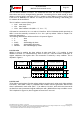
t
HDDAT
t
f
t
BUF
SDI
SCK
SDI
t
LOW
t
HDSTA
t
r
t
SUSTA
t
HIGH
t
SUDAT
t
SUSTO
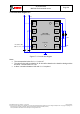
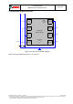
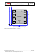
Figure 14: I²C timing diagram
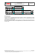
Table 33: I²C timings
Parameter
Symbol
Condition
Min
Typ
Max
Unit
SDI setup time
t
SU;DAT
S&F Mode
HS mode
160
30
ns
ns
SDI hold time
t
HD;DAT
S&F Mode, C
b
S&F Mode, C
b
HS mode, C
b
HS mode, C
b
80
90
18
24
115
150
ns
ns
ns
ns
SCK low pulse
t
LOW
HS mode, C
b
V
DDIO
= 1.62 V
160
ns
SCK low pulse
t
LOW
HS mode, C
b
V
DDIO
= 1.2 V
210
ns
The above-mentioned I
2
C specific timings correspond to the following internal added delays:
Input delay between SDI and SCK inputs: SDI is more delayed than SCK by typically
100 ns in Standard and Fast Modes and by typically 20 ns in High Speed Mode.
Output delay from SCK falling edge to SDI output propagation is typically 140 ns in
Standard and Fast Modes and typically 70 ns in High Speed Mode.
6.4.3 SPI timings
The SPI timing diagram is in Figure 15, while the corresponding values are given in Table 34.
All timings apply both to 4- and 3-wire SPI.