
Data Sheet

Final Datasheet
BME280 Environmental sensor
Page 34
BST-BME280-DS001-10 | Revision 1.1 | May 2015 Bosch Sensortec
© Bosch Sensortec GmbH reserves all rights even in the event of industrial property rights. We reserve all rights of disposal such as copying and passing on to
third parties. BOSCH and the symbol are registered trademarks of Robert Bosch GmbH, Germany.
Note: Specifications within this document are subject to change without notice.
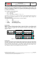
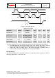
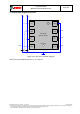
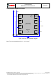
Start
RW Stop
1 1 1 1 0 1 1 0 bit15 bit14 bit13 bit12 bit11 bit10 bit9 bit8 bit7 bit6 bit5 bit4 bit3 bit2 bit1 bit0
CSB
=
1
Data byte
Data register - address F7h
Register address (F6h)
CSB
=
0
Control byte
Data byte
Data register - address F6h
Figure 13: SPI multiple byte read
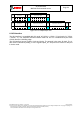
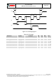
6.4 Interface parameter specification
6.4.1 General interface parameters
The general interface parameters are given in Table 32 below.
Table 32: interface parameters
Parameter
Symbol
Condition
Min
Typ
Max
Unit
Input low level
V
il_si
V
DDIO
=1.2 V to 3. 6V
20
%V
DDIO
Input high level
V
ih_si
V
DDIO
=1.2 V to 3.6 V
80
%V
DDIO
Output low level I
2
C
V
ol_SDI
V
DDIO
=1.62 V, I
ol
=3 mA
20
%V
DDIO
Output low level I
2
C
V
ol_SDI_1.2
V
DDIO
=1.20 V, I
ol
=3 mA
23
%V
DDIO
Output low level SPI
V
ol_SDO
V
DDIO
=1.62 V, I
ol
=1 mA
20
%V
DDIO
Output low level SPI
V
ol_SDO_1.2
V
DDIO
=1.20 V, I
ol
=1 mA
23
%V
DDIO
Output high level
V
oh
V
DDIO
=1.62 V, I
oh
=1 mA
(SDO, SDI)
80
%V
DDIO
Output high level
V
oh_1.2
V
DDIO
=1.20 V, I
oh
=1 mA
(SDO, SDI)
60
%V
DDIO
Pull-up resistor
R
pull
Internal CSB pull-up
resistance to V
DDIO
70
120
190
k
I
2
C bus load capacitor
C
b
On SDI and SCK
400
pF
6.4.2 I²C timings
For I²C timings, the following abbreviations are used:
C
b
= bus capacitance on SDA line
All other naming refers to I²C specification 2.1 (January 2000).
The I²C timing diagram is in Figure 14. The corresponding values are given in Table 33.