
Data Sheet

Final Datasheet
BME280 Environmental sensor
Page 33
BST-BME280-DS001-10 | Revision 1.1 | May 2015 Bosch Sensortec
© Bosch Sensortec GmbH reserves all rights even in the event of industrial property rights. We reserve all rights of disposal such as copying and passing on to
third parties. BOSCH and the symbol are registered trademarks of Robert Bosch GmbH, Germany.
Note: Specifications within this document are subject to change without notice.
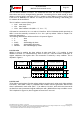
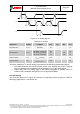
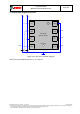
The SPI interface uses the following pins:
CSB: chip select, active low
SCK: serial clock
SDI: serial data input; data input/output in 3-wire mode
SDO: serial data output; hi-Z in 3-wire mode
Refer to chapter 7 for connection instructions.
CSB is active low and has an integrated pull-up resistor. Data on SDI is latched by the device at
SCK rising edge and SDO is changed at SCK falling edge. Communication starts when CSB
goes to low and stops when CSB goes to high; during these transitions on CSB, SCK must be
stable. The SPI protocol is shown in Figure 11. For timing details, please review Table 34.
CSB
SCK
SDI
RW
AD6
AD5
AD4
AD3
AD2
AD1
AD0
DI5
DI4
DI3
DI2
DI1
DI0
DI7
DI6
SDO
DO5
DO4
DO3
DO2
DO1
DO0
DO7
DO6
tri-state
Figure 11: -wire configuration)
In SPI mode, only 7 bits of the register addresses are used; the MSB of register address is not
or read).
Example: address 0xF7 is accessed by using SPI register address 0x77. For write access, the
byte 0x77 is transferred, for read access, the byte 0xF7 is transferred.
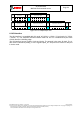
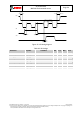
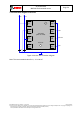
6.3.1 SPI write
Writing is done by lowering CSB and sending pairs control bytes and register data. The control
bytes consist of the SPI register address (= full register address without bit 7) and the write
command (. Several pairs can be written without raising CSB. The transaction is
ended by a raising CSB. The SPI write protocol is depicted in Figure 12.
Start
RW RW Stop
0 1 1 1 0 1 0 0 bit7 bit6 bit5 bit4 bit3 bit2 bit1 bit0 0 1 1 1 0 1 0 1 bit7 bit6 bit5 bit4 bit3 bit2 bit1 bit0
Control byte
CSB
=
1
Data byte
Register address (F5h)
Data register - adress F5h
Register address (F4h)
CSB
=
0
Control byte
Data byte
Data register - address F4h
Figure 12: SPI multiple byte write (not auto-incremented)
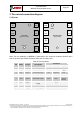
6.3.2 SPI read
Reading is done by lowering CSB and first sending one control byte. The control bytes consist
of the SPI register address (= full register address without bit 7) and the read command (bit 7 =
pin (SDI in 3-wire mode);
the register address is automatically incremented. The SPI read protocol is depicted in Figure
13.