
Data Sheet

Final Datasheet
BME280 Environmental sensor
Page 30
BST-BME280-DS001-10 | Revision 1.1 | May 2015 Bosch Sensortec
© Bosch Sensortec GmbH reserves all rights even in the event of industrial property rights. We reserve all rights of disposal such as copying and passing on to
third parties. BOSCH and the symbol are registered trademarks of Robert Bosch GmbH, Germany.
Note: Specifications within this document are subject to change without notice.
6. Digital interfaces
The BME280 supports the I²C and SPI digital interfaces; it acts as a slave for both protocols.
The I²C interface supports the Standard, Fast and High Speed modes. The SPI interface
011) in 4-
wire and 3-wire configuration.
The following transactions are supported:
Single byte write
multiple byte write (using pairs of register addresses and register data)
single byte read
multiple byte read (using a single register address which is auto-incremented)
6.1 Interface selection
Interface selection is done automatically based on CSB (chip select) status. If CSB is connected
to V
DDIO
, the I²C interface is active. If CSB is pulled down, the SPI interface is activated. After
CSB has been pulled down once (regardless of whether any clock cycle occurred), the I²C
interface is disabled until the next power-on-reset. This is done in order to avoid inadvertently
decoding SPI traffic to another slave as I²C data. Since the device startup is deferred until both
V
DD
and V
DDIO
are established, there is no risk of incorrect protocol detection because of the
power-up sequence used. However, if I²C is to be used and CSB is not directly connected to
V
DDIO
but is instead connected to a programmable pin, it must be ensured that this pin already
outputs the V
DDIO
level during power-on-reset of the device. If this is not the case, the device will
be locked in SPI mode and not respond to I²C commands.
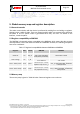
6.2 I²C Interface
The I²C slave interface is compatible with Philips I²C Specification version 2.1. For detailed
timings, please review Table 33. All modes (standard, fast, high speed) are supported. SDA and
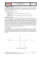
SCL are not pure open-drain. Both pads contain ESD protection diodes to VDDIO and GND. As
the devices does not perform clock stretching, the SCL structure is a high-Z input without drain
capability.
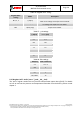
Figure 8: SDI/SCK ESD drawing