
Data Sheet

Final Datasheet
BME280 Environmental sensor
Page 24
BST-BME280-DS001-10 | Revision 1.1 | May 2015 Bosch Sensortec
© Bosch Sensortec GmbH reserves all rights even in the event of industrial property rights. We reserve all rights of disposal such as copying and passing on to
third parties. BOSCH and the symbol are registered trademarks of Robert Bosch GmbH, Germany.
Note: Specifications within this document are subject to change without notice.
((BME280_S32_t)dig_H3)) >> 11) + ((BME280_S32_t)32768))) >> 10) + ((BME280_S32_t)2097152)) *
((BME280_S32_t)dig_H2) + 8192) >> 14));
v_x1_u32r = (v_x1_u32r – (((((v_x1_u32r >> 15) * (v_x1_u32r >> 15)) >> 7) * ((BME280_S32_t)dig_H1)) >> 4));
v_x1_u32r = (v_x1_u32r < 0 ? 0 : v_x1_u32r);
v_x1_u32r = (v_x1_u32r > 419430400 ? 419430400 : v_x1_u32r);
return (BME280_U32_t)(v_x1_u32r>>12);
}
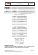
5. Global memory map and register description
5.1 General remarks
The entire communication with the device is performed by reading from and writing to registers.
Registers have a width of 8 bits. There are several registers which are reserved; they should not
be written to and no specific value is guaranteed when they are read. For details on the
interface, consult chapter 6.
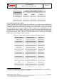
5.2 Register compatibility to BMP280
The BME280 is downward register compatible to the BMP280, which means that the pressure
and temperature control and readout is identical to BMP280. However, the following exceptions
have to be considered:
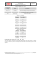
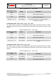
Table 17: Register incompatibilities between BMP280 and BME280
Register
Bits
Content
BMP280
BME280
id
7:0
chip_id
Read value is
0x56 / 0x57 (samples)
0x58 (mass production)
Read value is 0x60
config
7:5
t_sb
110: 2000 ms
111: 4000 ms
110: 10 ms
111: 20 ms
0xFpress
19:0
press
depends only on osrs_p
Without filter, resolution depends on
osrs_p; when using filter, resolution
is always 20 bit
0xFC temp
19:0
temp
only depends on osrs_t
Without filter, resolution depends on
osrs_t; when using filter, resolution is
always 20 bit
5.3 Memory map
The memory map is given in Table 18 below. Reserved registers are not shown.