
Data Sheet

Page 6 ams Datasheet
Document Feedback [v1-00] 2016-Dec-23
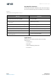
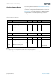
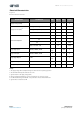
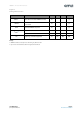
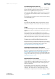
CCS811 − Elec trical Characteristics
Figure 6:
Electrical Characteristics
Note(s):
1. The supply voltage V
DD
is sampled during boot and should not vary during operation
2. The maximum V
DD
ramp time for Power On is 3ms
3. Typical values for 1.8V supply voltage (V
DD
)
4. Average Supply Current (I
DD
) for a sensor measurement once every 60 seconds
5. For SDA and SCL timing refer NXP I²C – bus specification and user manual UM10204
6. Typical values at 25
o
C and 50% RH
Parameters Conditions Min
Typ
(6)
Max Units
Supply Voltage (V
DD
)
(1), (2)
1.8 3.3 V
Supply Current (I
DD
)
(3)
During measuring at 1.8V 26 mA
Average over pulse cycle
(3)
at 1.8V
0.7 mA
Sleep Mode at 1.8V 19 µA
Power Consumption
Idle Mode 0 at V
DD
= 1.8V
0.034 mW
Mode 1 & 4 at V
DD
= 1.8V
46 mW
Mode 2 at V
DD
= 1.8V
7mW
Mode 3 at V
DD
= 1.8V
1.2 mW
Logic High Input
(5)
nRESET, nWAKE, ADDR
V
DD
-
0.6
V
DD
V
Logic Low Input
(5)
nRESET, nWAKE, ADDR 0 0.6 V
Logic High Output nINT
V
DD
-
0.7
V
Logic Low Output nINT 0.6 V
Analogue Input AUX 0
V
DD
V
Electrical Characteristics