
Data Sheet

Page 4 ams Datasheet
Document Feedback [v1-00] 2016-Dec-23
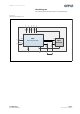
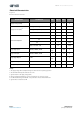
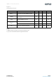
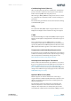
CCS811 − Pin Assignment
Figure 3:
Pin Diagram
Pin Diagram: The Exposed Pad is underneath
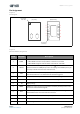
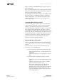
Figure 4:
CCS811 LGA Pin Assignment
Pin No. Pin Name Description
1 ADDR
Single address select bit to allow alternate address to be selected
• When ADDR is low the 7 bit I²C address is decimal 90 / hex 0x5A
• When ADDR is high the 7 bit I²C address is decimal 91 / hex 0x5B.
2nRESET
nRESET is an active low input and is pulled up to V
DD
by default. nRESET is
optional but external 4.7KΩ pull-up and/or decoupling of the nRESET pin may be
necessary to avoid erroneous noise-induced resets.
3nINT
nINT is an active low optional output. It is pulled low by the CCS811 to indicate
end of measurement or a set threshold value has been triggered.
4 PWM Heater driver PWM output. Pins 4 and 5 must be connected together.
5 Sense Heater current sense. Pins 4 and 5 must be connected together.
6
V
DD
Supply voltage
7nWAKE
nWAKE is an active low input and should be asserted by the host prior to an I²C
transaction and held low throughout.
8AUX
Optional AUX pin which can be used for ambient temperature sensing with an
external NTC resistor. If not used leave unconnected.
9SDA
SDA pin is used for I²C data. Should be pulled up to V
DD
with a resistor
10 SCL
SCL pin is used for I²C clock. Should be pulled up to V
DD
with a resistor
EP Exposed Pad Connect to ground
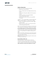
Pin Assignment
Pin 1 Corner
Index Area
(Top View)
Pin 1 Corner
Index Area
(Bottom View)
1
5
10
6
7
8
9
4
3
2