
Data Sheet


ams Datasheet Page 27
[v1-00] 2016-Dec-23 Document Feedback
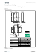
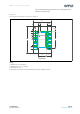
CCS811 − Package Drawings & Marking
The recommended package footprint or landing pattern for
CCS811 is shown below:
Figure 25:
Recommended Package Footprint for CCS811
Note(s):
1. All dimensions are in millimeters.
2. PCB land pattern in Green dash lines
3. Pin numbers are in Red
4. Add 0.05mm all around the nominal lead width and length for the PCB land pattern
4
0.6
1.3
0.6
2.7
0.4
0.4
5
1
6
10
(Top View)
0.75
0.7
0.3
0.3