CCS811 Ultra-Low Power Digital Gas Sensor for Monitoring Indoor Air Quality General Description The CCS811 is an ultra-low power digital gas sensor solution which integrates a metal oxide (MOX) gas sensor to detect a wide range of Volatile Organic Compounds (VOCs) for indoor air quality monitoring with a microcontroller unit (MCU), which includes an Analog-to-Digital converter (ADC), and an I²C interface.
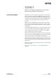
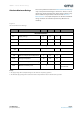
CCS811 − General Description Key Benefits & Features The benefits and features of CCS811, Ultra-Low Power Digital Gas Sensor for Monitoring Indoor Air Quality are listed below: Figure 1: Added Value of Using CCS811 Sensor Benefits Features • Manages the sensor drive modes and measurements while detecting VOCs • Integrated MCU • Provides eCO2 level or TVOC indication with no host intervention • On-board processing • Simplifies the hardware and software integration • Standard I²C digital interface •
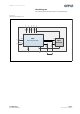
CCS811 − General Description Block Diagram The functional blocks of this device are shown below: Figure 2: CCS811 Block Diagram VDD SDA 6 10 SCL 9 1 ADDR AUX 8 H+ 3 S+ (With Integrated ADC) nRESET 7 ams Datasheet [v1-00] 2016-Dec-23 EP 4 Sense PWM GND H- nWAKE 2 MCU nINT MOX Gas Sensor S- 5 Page 3 Document Feedback
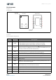
CCS811 − Pin Assignment Pin Assignment Figure 3: Pin Diagram Pin 1 Corner Index Area (Bottom View) (Top View) 5 6 4 7 3 2 8 9 1 10 Pin 1 Corner Index Area Pin Diagram: The Exposed Pad is underneath Figure 4: CCS811 LGA Pin Assignment Pin No. Pin Name 1 ADDR 2 nRESET 3 nINT nINT is an active low optional output. It is pulled low by the CCS811 to indicate end of measurement or a set threshold value has been triggered. 4 PWM Heater driver PWM output.
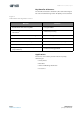
CCS811 − Absolute Maximum Ratings Absolute Maximum Ratings Stresses beyond those listed under Absolute Maximum Ratings may cause permanent damage to the device. These are stress ratings only. Functional operation of the device at these or any other conditions beyond those indicated under Electrical Characteristics is not implied. Exposure to absolute maximum rating conditions for extended periods may affect device reliability Figure 5: Absolute Maximum Ratings Symbol Parameter Min Max Units 3.
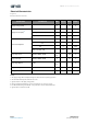
CCS811 − Electrical Characteristics Electrical Characteristics Figure 6: Electrical Characteristics Parameters Conditions Min Supply Voltage (VDD) (1), (2) Supply Current (IDD) (3) Typ (6) 1.8 Max Units 3.3 V During measuring at 1.8V 26 mA Average over pulse cycle(3) at 1.8V 0.7 mA Sleep Mode at 1.8V 19 μA Idle Mode 0 at VDD= 1.8V 0.034 mW Mode 1 & 4 at VDD= 1.8V 46 mW Mode 2 at VDD= 1.8V 7 mW Mode 3 at VDD= 1.8V 1.
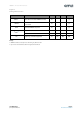
CCS811 − Electrical Characteristics Figure 7: Timing Characteristics Parameters Conditions Min Typ Max Units Time until active after nWAKE asserted. 50 μs tDWAKE Minimum time nWAKE should be de-asserted 20 μs tRESET Minimum nRESET low pulse 20 μs tAWAKE (1) Time until active after Power on 18 20 ms Time until active after nRESET 1 2 ms 100 400 kHz tSTART (2) fI²C Frequency of I²C Bus Supported 10 Note(s): 1.
CCS811 − Detailed Description Detailed Description Modes of Operation The CCS811 has 5 modes of operation as follows • Mode 0: Idle, low current mode • Mode 1: Constant power mode, IAQ measurement every second • Mode 2: Pulse heating mode IAQ measurement every 10 seconds • Mode 3: Low power pulse heating mode IAQ measurement every 60 seconds • Mode 4: Constant power mode, sensor measurement every 250ms In Modes 1, 2, 3, the equivalent CO 2 concentration (ppm) and TVOC concentration (ppb) are calculated for
CCS811 − Detailed Description Conditioning Period (Run-In) After early-life (Burn-In) period is complete the conditioning period is the time required to achieve good sensor stability before measuring VOCs after long idle period. After writing to MEAS_MODE to configure the sensor in mode 1-4, run CCS811 for 20 minutes, before accurate readings are generated. The conditioning period must also be observed before writing to the BASELINE register.
CCS811 − Detailed Description Refer to application note ams AN000372 for more details on NTC configuration. If an external temperature sensor is not available the external NTC circuit can be used to determine the ambient temperature and write this information to CCS811. The NTC Register provides the voltages across the R NTC and the R REF if fitted (mV) – to enable host system to calculate the ambient temperature.
CCS811 − Detailed Description Note(s): 1. If a value is written to the BASELINE register while the sensor is stabilising, the output of the TVOC and eCO 2 calculations may be higher than expected. 2. The baseline must be written after the conditioning period For additional information on using the CCS811 please refer to application note ams AN000369: CCS811 Programming and Interfacing Guide.
CCS811 − Application Information Application Information The recommended application circuit for CCS811 is shown below. Figure 8: Recommended Application Circuit VDD 4K7 Part of host system Host Processor 4K7 VDD 6 CCS811 Digital VOC sensor SCL SCL SDA SDA GPIOx nWAKE ADDR ADDR 1uF GND Note(s): 1. Pull-up resistors for SCL and SDA assumed will be part of host system. 2. AUX Pin on CCS811 can be used for optional ambient temperature sensing, if not used leave unconnected. 3.
CCS811 − Application Information I²C Interface I²C transactions require a register address to be selected (written) and followed by data, as described by the transaction types in the subsections below. Each Register location corresponds to a byte or multiple bytes. Multiple reads or writes in a single sequence will be to or from the same location (the address does not increment). Therefore, registers are sometimes referred to as mailboxes in this document.
CCS811 − Application Information I²C Register Read Figure 10: I²C Register Read Select and read register value Select and read register value, as single transaction Select and repeatedly read multiple data values from register S SLAVE ADDRESS W A DATA(REG ADDR) A P (select register address) S SLAVE ADDRESS R A DATA N P (read register value) S SLAVE ADDRESS W A DATA(REG ADDR) A S SLAVE ADDRESS (select register address) R A DATA N P (read register value) A P (select register addre
CCS811 − Application Register Overview Application Register Overview All I²C transactions must use the (7 bits) slave address 0x5A or 0x5B depending on status of ADDR pin when writing to and reading from the CCS811. Figure 11 shows the register map for CCS811. Figure 23 shows the bootloader register map.
CCS811 − Application Register Overview STATUS Register (0x00) Single byte read only register which indicates if a device is active, if new data is available or if an error occurred. Figure 12: Status Register 7 6 FW_MODE 5 - Bit(s) Field 7 FW_MODE 6:5 - 4 APP_VALID 3 DATA_READY 2:1 - 0 ERROR Page 16 Document Feedback 4 3 APP_VALID DATA_READY 2 1 - 0 ERROR Description 0: Firmware is in boot mode, this allows new firmware to be loaded 1: Firmware is in application mode.
CCS811 − Application Register Overview MEAS_MODE (Measurement and Conditions) Register (0x01) This is Single byte register, which is used to enable sensor drive mode and interrupts.
CCS811 − Application Register Overview ALG_RESULT_DATA (Algorithm Results Data) Register (0x02) This multi-byte read only register contains the calculated eCO 2 (ppm) and TVOC (ppb) values followed by the STATUS register, ERROR_ID register and the RAW_DATA register. • If only eCO 2 is required, only the first 2 bytes need to be read. • If TVOC is required, 4 bytes need to be read.
CCS811 − Application Register Overview ENV_DATA (Environment Data) Register (0x05) A multi-byte register that can be written with the current Humidity and Temperature values if known.
CCS811 − Application Register Overview NTC Register (0x06) Four byte read only register which contains the voltage across resistor (R REF) and the voltage across the NTC resistor from which the ambient temperature can be determined. The resistance of the NTC resistor can be determined by the ratio value and knowledge of the reference resistor used. R NTC = VNTC x R REF / VREF. The temperature can be determined from the resistance of the NTC resistor from the datasheet of the NTC resistor used.
CCS811 − Application Register Overview BASELINE Register (0x11) A two byte read/write register which contains an encoded version of the current baseline used in Algorithm Calculations. A previously stored value may be written back to this two byte register and the Algorithms will use the new value in its calculations (until it adjusts it as part of its internal Automatic Baseline Correction).
CCS811 − Application Register Overview FW_App_Version (Firmware Application Version) Register (0x24) Two byte read only register which contain the version of the firmware application stored in the CCS811 in the format Major.Minor.
CCS811 − Application Register Overview SW_RESET Register (0xFF) As an alternative to Power-On reset or Hardware Reset a Software Reset is available. Asserting the SW_RESET will restart the CCS811 in Boot mode to enable new application firmware to be downloaded. To prevent accidental SW_RESET a sequence of four bytes must be written to this register in a single I²C sequence: 0x11, 0xE5, 0x72, 0x8A. For details, please refer to application notes ams AN000369 and ams AN000371.
CCS811 − Bootloader Register Over view Bootloader Register Overview All I²C transactions must use the (7bits) slave address 0x5A or 0x5B depending on status of ADDR pin when writing to and reading from the CCS811. Figure 23 shows the bootloader register map for CCS811. Figure 23: CCS811 Bootloader Register Map Address Register R/W Size Description 0x00 STATUS R 1 byte Status register 0x20 HW_ID R 1 byte Hardware ID. The value is 0x81 0x21 HW Version R 1 byte Hardware Version.
CCS811 − Bootloader Register Overview Registers not detailed below are documented in the Application Register Overview section. APP_ERASE (Application Erase) Register (0xF1) To prevent accidental APP_ERASE a sequence of four bytes must be written to this register in a single I²C sequence: 0xE7, 0xA7, 0xE6, 0x09. The APP_ERASE can take a variable amount of time. The status register can be polled to determine when this function is complete.
CCS811 − Package Drawings & Mark ing Package Drawings & Marking LGA Package Outline Figure 24: LGA Package Drawings Pin 1 Corner Index Area (Top View) (Side View) D A E 1.2 nxL nxW 6 5 e D1 2.4 1 Pin 1 Corner Index Area RoHS 10 (0.3) Green E1 (Bottom View) Symbol Total thickness Body Size Lead Width Lead Length Lead Pitch Lead Count Edge Lead Centre to Centre A D E W L e n D1 E1 Min - 0.25 0.45 Dimensions Nominal 4.0 2.7 0.3 0.5 0.6 10 2.4 2.2 Max 1.1 BSC BSC 0.35 0.
CCS811 − Package Drawings & Marking The recommended package footprint or landing pattern for CCS811 is shown below: Figure 25: Recommended Package Footprint for CCS811 2.7 0.6 0.3 0.75 1 10 0.3 0.4 0.6 4 0.4 5 6 1.3 0.7 (Top View) Note(s): 1. All dimensions are in millimeters. 2. PCB land pattern in Green dash lines 3. Pin numbers are in Red 4. Add 0.
CCS811 − Package Drawings & Mark ing Product Marking Figure 26: Package Marking Note(s): 1. Product code is 811B 2.
CCS811 − Ordering & Contact Information Ordering & Contact Information Figure 27: Ordering Information Ordering Code Description Package MOQ CCS811B-JOPR CCS811 digital gas sensor for Indoor Air Quality Monitoring 2.7mm x 4.0mm x 1.1mm LGA 5000 CCS811B-JOPD Sample of CCS811 digital gas sensor for Indoor Air Quality Monitoring 2.7mm x 4.0mm x 1.1mm LGA 500 Note(s): 1. Refer to JEDEC J-STD020 lead-free standard for typical soldering reflow profile Technical Support is available at: www.ams.
CCS811 − RoHS Compliant & ams Green Statement RoHS Compliant & ams Green Statement RoHS: The term RoHS compliant means that ams AG products fully comply with current RoHS directives. Our semiconductor products do not contain any chemicals for all 6 substance categories, including the requirement that lead not exceed 0.1% by weight in homogeneous materials. Where designed to be soldered at high temperatures, RoHS compliant products are suitable for use in specified lead-free processes.
CCS811 − Copyrights & Disclaimer Copyrights & Disclaimer Copyright ams AG, Tobelbader Strasse 30, 8141 Premstaetten, Austria-Europe. Trademarks Registered. All rights reserved. The material herein may not be reproduced, adapted, merged, translated, stored, or used without the prior written consent of the copyright owner. Devices sold by ams AG are covered by the warranty and patent indemnification provisions appearing in its General Terms of Trade.
CCS811 − Document Status Document Status Document Status Product Preview Preliminary Datasheet Datasheet Datasheet (discontinued) Page 32 Document Feedback Product Status Definition Pre-Development Information in this datasheet is based on product ideas in the planning phase of development.
CCS811 − Revision Information Revision Information Changes from CCMOSS version 7B (2016-Oct-06) to current revision 1-00 (2016-Dec-23) Page Content of CCMOS Sensors datasheet was updated to the latest ams design Completely revised version Note(s): 1. Page and figure numbers for the previous version may differ from page and figure numbers in the current revision. 2. Correction of typographical errors is not explicitly mentioned.
CCS811 − Appendix Appendix References Figure 28: Document Reference Document Reference Description ams AN000367 Assembly guidelines for CCS811 ams AN000368 Mechanical considerations for CCS811 ams AN000369 CCS811 programming and interfacing guide ams AN000370 CCS811 Clean Air Baseline Save and Restore ams AN000371 CCS811 Performing a Firmware download ams AN000372 Connecting an NTC Thermistor to the CCS811 ams AN000373 CCS811 Manufacture Test Procedure ams WP000102 IAQ User experience dur
CCS811 − Content Guide Content Guide 1 2 2 3 General Description Key Benefits & Features Applications Block Diagram 4 5 6 Pin Assignment Absolute Maximum Ratings Electrical Characteristics 8 8 8 9 9 9 9 9 9 10 10 Detailed Description Modes of Operation Early-Life Use (Burn-In) Conditioning Period (Run-In) eCO2 TVOC Temperature and Humidity Compensation Interrupt and Interrupt on Threshold Optional NTC Circuit (AUX) Automatic Baseline Correction Manual Baseline Correction 12 12 13 13 14 Application
CCS811 − Content Guide Page 36 Document Feedback 26 26 28 Package Drawings & Marking LGA Package Outline Product Marking 29 30 31 32 33 Ordering & Contact Information RoHS Compliant & ams Green Statement Copyrights & Disclaimer Document Status Revision Information 34 34 Appendix References ams Datasheet [v1-00] 2016-Dec-23