
Data Sheet

High Accuracy, Galvanically Isolated Current Sensor IC
With Small Footprint SOIC8 Package
ACS723
20
Allegro MicroSystems, LLC
115 Northeast Cutoff
Worcester, Massachusetts 01615-0036 U.S.A.
1.508.853.5000; www.allegromicro.com
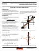
DEFINITIONS OF DYNAMIC RESPONSE CHARACTERISTICS
Power-On Time (t
PO
)
When the supply is ramped to its operating voltage, the device
requires a finite time to power its internal components before
responding to an input magnetic field.
Power-On Time, t
PO
, is defined as the time it takes for the output
voltage to settle within ±10% of its steady state value under an
applied magnetic field, after the power supply has reached its
minimum specified operating voltage, V
CC
(min), as shown in the
chart at right.
Rise Time (t
r
)
The time interval between a) when the sensor IC reaches 10% of
its full scale value, and b) when it reaches 90% of its full scale
value. The rise time to a step response is used to derive the band-
width of the current sensor IC, in which ƒ(–3 dB) = 0.35 / t
r
. Both
t
r
and t
RESPONSE
are detrimentally affected by eddy current losses
observed in the conductive IC ground plane.
Propagation Delay (t
pd
)
The propagation delay is measured as the time interval a) when
the primary current signal reaches 20% of its final value, and b)
when the device reaches 20% of its output corresponding to the
applied current.
Response Time (t
RESPONSE
)
The time interval between a) when the primary current signal
reaches 90% of its final value, and b) when the device reaches
90% of its output corresponding to the applied current.
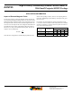
V
IOUT
V
t
V
CC
V
CC
(min.)
90% V
IOUT
0
t
1
= time at which power supply reaches
minimum specified operating voltage
t
2
=
time at which output voltage settles
within ±10% of its steady state value
under an applied magnetic field
t
1
t
2
t
PO
V
CC
(typ.)
Primary Current
V
IOUT
90
0
(%)
Response Time, t
RESPONSE
t
Primary Current
V
IOUT
90
10
20
0
(%)
Propagation Delay, t
pd
Rise Time, t
r
t
Figure 3: Power-On Time (t
PO
)
Figure 4: Rise Time (t
r
) and Propagation Delay (t
pd
)
Figure 5: Response Time (t
RESPONSE
)