
Data Sheet

Digital interfaces LSM9DS1
34/72 DocID025715 Rev 2
5.3 Magnetic sensor SPI bus interface
The LSM9DS1 magnetic sensor SPI is a bus slave. The SPI allows writing and reading the
registers of the device.
The serial interface connects to applications using 4 wires: CS_M, SPC, SDI and SDO_M.
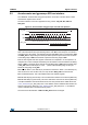
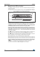
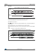
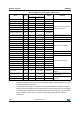
Figure 22. Magnetic sensor read and write protocol
CS_M is the serial port enable and it is controlled by the SPI master. It goes low at the start
of the transmission and goes back high at the end. SPC is the serial port clock and it is
controlled by the SPI master. It is stopped high when CS_M is high (no transmission). SDI
and SDO_M are respectively the serial port data input and output. Those lines are driven at
the falling edge of SPC and should be captured at the rising edge of SPC.
Both the read register and write register commands are completed in 16 clock pulses or in
multiples of 8 in case of multiple read/write bytes. Bit duration is the time between two falling
edges of SPC. The first bit (bit 0) starts at the first falling edge of SPC after the falling edge
of CS_M while the last bit (bit 15, bit 23, ...) starts at the last falling edge of SPC just before
the rising edge of CS_M.
bit 0: RW bit. When 0, the data DI(7:0) is written into the device. When 1, the data DO(7:0)
from the device is read. In latter case, the chip will drive SDO_M at the start of bit 8.
bit 1: MS bit. When 0, the address will remain unchanged in multiple read/write commands.
When 1, the address is auto-incremented in multiple read/write commands.
bit 2-7: address AD(5:0). This is the address field of the indexed register.
bit 8-15: data DI(7:0) (write mode). This is the data that is written into the device (MSb first).
bit 8-15: data DO(7:0) (read mode). This is the data that is read from the device (MSb first).
In multiple read/write commands further blocks of 8 clock periods will be added. When the
MS bit is ‘0’, the address used to read/write data remains the same for every block. When
the MS bit is ‘1’, the address used to read/write data is increased at every block.
The function and the behavior of SDI and SDO_M remain unchanged.
CS
SPC
SDI
SDO
RW
AD5 AD4 AD3 AD2 AD1 AD0
DI7 DI6 DI5 DI4 DI3 DI2 DI1 DI0
DO7DO6DO5DO4DO3DO2DO1DO0
MS
AM10129V1
CS_M
SDO_M