
Data Sheet

Digital interfaces LSM9DS1
32/72 DocID025715 Rev 2
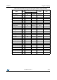
5.2.1 SPI read
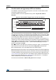
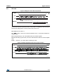
Figure 17. Accelerometer and gyroscope SPI read protocol
The SPI read command is performed with 16 clock pulses. A multiple byte read command is
performed by adding blocks of 8 clock pulses to the previous one.
bit 0: READ bit. The value is 1.
bit 1-7: address AD(6:0). This is the address field of the indexed register.
bit 8-15: data DO(7:0) (read mode). This is the data that will be read from the device (MSb
first).
bit 16-... : data DO(...-8). Further data in multiple byte reads.
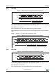
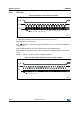
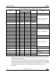
Figure 18. Multiple byte SPI read protocol (2-byte example)
5.2.2 SPI write
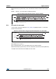
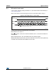
Figure 19. Accelerometer and gyroscope SPI write protocol
The SPI write command is performed with 16 clock pulses. A multiple byte write command
is performed by adding blocks of 8 clock pulses to the previous one.
bit 0: WRITE bit. The value is 0.
bit 1 -7: address AD(6:0). This is the address field of the indexed register.
CS
SPC
SDI
SDO
RW
DO7 DO6 DO5 DO4 DO3 DO2 DO1 DO0
AD5 AD4 AD3 AD2 AD1 AD0AD6
CS_A/G
SDO_A/G
CS
SPC
SDI
SDO
RW
DO7 DO6 DO5 DO4 DO3 DO2 DO1 DO0
AD5 AD4 AD3 AD2 AD1 AD0
8OD9OD 01OD 11OD 21OD 31OD 41OD 51OD
AD6
CS_A/G
SDO_A/G
CS
SPC
SDI
RW
DI7 DI6 DI5 DI4 DI3 DI2 DI1 DI0
AD5 AD4 AD3 AD2 AD1 AD0AD6
CS_A/G