
Data Sheet

DocID025715 Rev 2 17/72
LSM9DS1 Module specifications
72
2.5 Absolute maximum ratings
Stresses above those listed as “Absolute maximum ratings” may cause permanent damage
to the device. This is a stress rating only and functional operation of the device under these
conditions is not implied. Exposure to maximum rating conditions for extended periods may
affect device reliability.
Note: Supply voltage on any pin should never exceed 4.8 V.
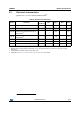
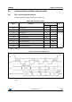
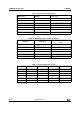
Table 8. Absolute maximum ratings
Symbol Ratings Maximum value Unit
Vdd Supply voltage -0.3 to 4.8 V
Vdd_IO I/O pins supply voltage -0.3 to 4.8 V
Vin
Input voltage on any control pin
(including CS_A/G, CS_M, SCL/SPC, SDA/SDI/SDO,
SDO_A/G, SDO_M)
0.3 to Vdd_IO +0.3 V
A
UNP
Acceleration (any axis)
3,000 for 0.5 ms g
10,000 for 0.1 ms g
M
EF
Maximum exposed field 1000 gauss
ESD Electrostatic discharge protection (HBM) 2 kV
T
STG
Storage temperature range -40 to +125 °C
This device is sensitive to mechanical shock, improper handling can cause
permanent damage to the part.
This device is sensitive to electrostatic discharge (ESD), improper handling can
cause permanent damage to the part.