
Data Sheet

DocID025715 Rev 2 15/72
LSM9DS1 Module specifications
72
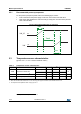
2.4 Communication interface characteristics
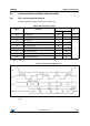
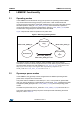
2.4.1 SPI - serial peripheral interface
Subject to general operating conditions for Vdd and Top.
Figure 3. SPI slave timing diagram
Note: Measurement points are done at 0.2·Vdd_IO and 0.8·Vdd_IO, for both input and output
ports.
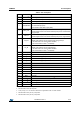
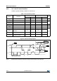
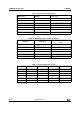
Table 6. SPI slave timing values
Symbol Parameter
Value
(1)
Unit
Min Max
t
c(SPC)
SPI clock cycle 100 ns
f
c(SPC)
SPI clock frequency 10 MHz
t
su(CS)
CS setup time 5
ns
t
h(CS)
CS hold time 20
t
su(SI)
SDI input setup time 5
t
h(SI)
SDI input hold time 15
t
v(SO)
SDO valid output time 50
t
h(SO)
SDO output hold time 5
t
dis(SO)
SDO output disable time 50
1. Values are guaranteed at 10 MHz clock frequency for SPI with both 4 and 3 wires, based on characterization results, not
tested in production