
Data Sheet
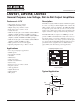

DATA SHEET LMV321/LMV358/LMV324
4
REV. 1D. Feb. 2012
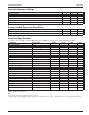
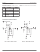
Electrical Specifications
(T
c
= 25°C, V
s
= +5V, G = 2, R
L
= 10kΩ to V
s
/2, R
f
= 10kΩ, V
o (DC)
= V
cc
/2; unless otherwise noted)
Parameter Conditions Min. Typ. Max. Unit
AC Performance
Gain Bandwidth Product C
L
= 50pF, R
L
=2kΩ to V
s
/2 1.4 MHz
Phase Margin 73 deg
Gain Margin 12 dB
Slew Rate 1.5 V/µs
Input Voltage Noise >50kHz 33 nV/√Hz
Crosstalk: LMV358 100kHz 91 dB
LMV324 100kHz 80 dB
DC Performance
Input Offset Voltage
1
17mV
Average Drift 6 µV/°C
Input Bias Current
2
<1 nA
Input Offset Current
2
<1 nA
Power Supply Rejection Ratio
1
DC 50 65 dB
Open Loop Gain
1
50 70 dB
Supply Current (Per Channel)
1
100 150 µA
Input Characteristics
Input Common Mode Voltage Range
1
LO 0 -0.4 V
HI 3.8 3.6 V
Common Mode Rejection Ratio
1
50 75 dB
Output Characteristics
Output Voltage Swing R
L
= 2kΩ to V
s
/2; LO/HI 0.036 to 4.95 V
R
L
= 10kΩ to V
s
/2; LO
1
0.1 0.013 V
R
L
= 10kΩ to V
s
/2; HI
1
4.98 4.9 V
Short Circuit Output Current
1
sourcing; V
o
= 0V 5 +34 mA
sinking; V
o
= 5V 10 -23 mA
Min/max ratings are based on product characterization and simulation. Individual parameters are tested as noted. Outgoing quality levels are
determined from tested parameters.
Notes:
1. Guaranteed by testing or statistical analysis at +25°C.
2. +IN and -IN are gates to CMOS transistors with typical input bias current of <1nA. CMOS leakage is too small to practically measure.
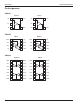
Package Thermal Resistance
Package θ
JA
5 lead SC70 331.4°C/W
5 lead SOT23 256°C/W
8 lead SOIC 152°C/W
8 lead MSOP 206°C/W
14 lead SOIC 88°C/W