
Design Guide


A DIVISION OF TRIMBLE
3
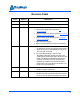
Revision Table
Date Version Description
3/2015 01 Draft 1 Partial Draft for early-access release
4/2015 01 REV A First Release for prototype units with 1.3.1 firmware
4/2015 01 Rev B Second release for GA units with version 1.3.2 firmware
Receive sensitivity values updated (RF
Characteristics)
Long-term exposure caution updated (ThingMagic
Nano Regulatory Information)
Thermal limits explained more fully (ThingMagic
Nano Carrier Board)
Minor Editorial Changes
Minor changes following review by Engineering
6/2015 01 Rev C
In the “Hardware Overview” section, the table of
pin fumctions erroneously listed pin 39 as both a
signal and a ground and omitted ground pin 37.
This has been corrected.
The “Host Board Design” section of the
“Hardware Integration chapter changed. The
“landing pads” outline changed to show heat sink
areas. The table that indicated pad sizes and
locations incorrectly has been removed and
replaced by a reference to the carrier board
design files, w hich provide the information in a
much more convenient form.
9/2015 01 Rev D
Ambiguity about whether RX and TX pins are
inputs or outputs cleared up.
4/2016 01 Rev E
Content added to reinforce that all GPI lines and
the RX input line must be low when the module
boots up and low when the module shuts down.