
Data Sheet


Bosch Sensortec | BME280 Data sheet
36 | 55
Modifications reserved | Data subject to change without notice
Document number: BST-BME280-DS002-15
Revision_1.6_092018
t
HDDAT
t
f
t
BUF
SDI
SCK
SDI
t
LOW
t
HDSTA
t
r
t
SUSTA
t
HIGH
t
SUDAT
t
SUSTO
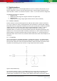
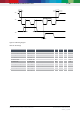
Figure 14: I²C timing diagram
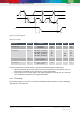
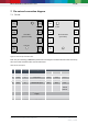
Table 33: I²C timings
Parameter
Symbol
Condition
Min
Typ
Max
Unit
SDI setup time
t
SU;DAT
S&F Mode
HS mode
160
30
ns
ns
SDI hold time
t
HD;DAT
S&F Mode, C
b
≤100 pF
S&F Mode, C
b
≤400 pF
HS mode, C
b
≤100 pF
HS mode, C
b
≤400 pF
80
90
18
24
115
150
ns
ns
ns
ns
SCK low pulse
t
LOW
HS mode, C
b
≤100 pF
V
DDIO
= 1.62 V
160
ns
SCK low pulse
t
LOW
HS mode, C
b
≤100 pF
V
DDIO
= 1.2 V
210
ns
The above-mentioned I
2
C specific timings correspond to the following internal added delays:
Input delay between SDI and SCK inputs: SDI is more delayed than SCK by typically 100 ns in
Standard and Fast Modes and by typically 20 ns in High Speed Mode.
Output delay from SCK falling edge to SDI output propagation is typically 140 ns in Standard
and Fast Modes and typically 70 ns in High Speed Mode.
6.4.3 SPI timings
The SPI timing diagram is in Figure 15, while the corresponding values are given in Table 34. All timings
apply both to 4- and 3-wire SPI.