
Data Sheet


Bosch Sensortec | BME280 Data sheet
33 | 55
Modifications reserved | Data subject to change without notice
Document number: BST-BME280-DS002-15
Revision_1.6_092018
BMP280’s I²C address. The SDO pin cannot be left floating; if left floating, the I²C address will be
undefined.
The I²C interface uses the following pins:
SCK: serial clock (SCL)
SDI: data (SDA)
SDO: Slave address LSB (GND = ‘0’, V
DDIO
= ‘1’)
CSB must be connected to V
DDIO
to select I²C interface. SDI is bi-directional with open drain to GND: it
must be externally connected to V
DDIO
via a pull up resistor. Refer to chapter 7 for connection
instructions.
The following abbreviations will be used in the I²C protocol figures:
S Start
P Stop
ACKS Acknowledge by slave
ACKM Acknowledge by master
NACKM Not acknowledge by master
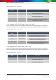
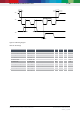
6.2.1 I²C write
Writing is done by sending the slave address in write mode (RW = ‘0’), resulting in slave address
111011X0 (‘X’ is determined by state of SDO pin. Then the master sends pairs of register addresses
and register data. The transaction is ended by a stop condition. This is depicted in Figure 9.
Start RW ACKS ACKS ACKS
1 1 1 0 1 1 X 0 1 0 1 0 0 0 0 0 bit7 bit6 bit5 bit4 bit3 bit2 bit1 bit0
…
ACKS ACKS Stop
…
1 0 1 0 0 0 0 1 bit7 bit6 bit5 bit4 bit3 bit2 bit1 bit0
Register data - address A0h
Register address (A0h)
Register address (A1h)
S
Slave Address
Control byte
Data byte
Control byte
Data byte
P
Register data - address A1h
Figure 9: I²C multiple byte write (not auto-incremented)
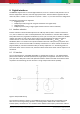
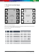
6.2.2 I²C read
To be able to read registers, first the register address must be sent in write mode (slave address
111011X0). Then either a stop or a repeated start condition must be generated. After this the slave is
addressed in read mode (RW = ‘1’) at address 111011X1, after which the slave sends out data from
auto-incremented register addresses until a NOACKM and stop condition occurs. This is depicted in
Figure 10, where register 0xF6 and 0xF7 are read.
Start RW ACKS ACKS
1 1 1 0 1 1 X 0 1 1 1 1 0 1 1 0
Start RW ACKS ACKM NOACKM Stop
1 1 1 0 1 1 X 1 bit7 bit6 bit5 bit4 bit3 bit2 bit1 bit0 bit7 bit6 bit5 bit4 bit3 bit2 bit1 bit0
Control byte
Data byte
Data byte
Register address (F6h)
S
Slave Address
P
S
Slave Address
Register data - address F7h
Register data - address F6h
Figure 10: I²C multiple byte read