
User Manual


VEML6030
www.vishay.com
Vishay Semiconductors
Rev. 1.3, 12-May-17
6
Document Number: 84366
For technical questions, contact: sensorstechsupport@vishay.com
THIS DOCUMENT IS SUBJECT TO CHANGE WITHOUT NOTICE. THE PRODUCTS DESCRIBED HEREIN AND THIS DOCUMENT
ARE SUBJECT TO SPECIFIC DISCLAIMERS, SET FORTH AT www.vishay.com/doc?91000
APPLICATION INFORMATION
VEML6030 is a cost effective solution of ambient light sensor with I
2
C bus interface. The standard serial digital interface is easy
to access “Ambient Light Signal” without complex calculation and programming by external controller. Beside the digital output
also a flexible programmable interrupt pin is available.
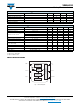
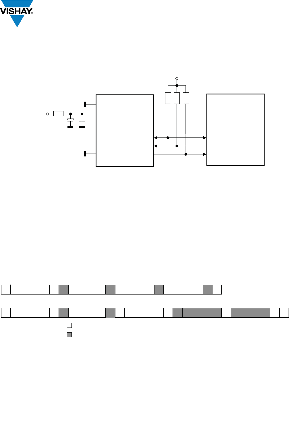
1. Application Circuit
Fig. 9 - Application Circuit
(x) = Pin Number
Notes
• The interrupt pin is an open drain output. Proposed values for the pull-up resistors should be > 1 kΩ, e.g. 2.2 kΩ to 4.7 kΩ for the R1 and
R2 (at SDA and SCL) and 10 kΩ to 100 kΩ for R3 (at interrupt).
Normally just one decoupling capacitor is needed. This should be ≥ 100 nF and placed close to the V
DD
pin.
Pin ADDR allows for the device addresses: pin 4 = high (V
DD
) = 0x48, pin 4 = low (GND) = 0x10
For detailed description about set-up and use of the interrupt as well as more application related information see AN: “Designing VEML6030
into an Application”
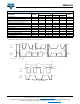
2. I
2
C Interface
The VEML6030 contains actual six 16 bit command codes for operation control, parameter setup, and result buffering. All
registers are accessible via I
2
C communication. Figure 7 shows the basic I
2
C communication with VEML6030.
The built in I
2
C interface is compatible with I
2
C modes “standard” and “fast”: 10 kHz to 400 kHz.
I
2
C H-level range = 1.3 V to 3.6 V.
Please refer to the I
2
C specification from NXP for details.
Fig. 10 - Send Byte / Receive Byte Protocol
Device Address
The VEML6030 has two fix slave addresses for the host
programming and accessing selection.
With ADDR pin plugged to power supply = high = V
DD
, the
predefined 7 bit I2C bus address is set to 1001000 = 0x48.
The least significant bit (LSB) defines read or write mode.
Accordingly the bus address is set to 1001 0000 = 90h for
write and 1001 0001 = 91h for read.
With ADDR pin plugged to ground = low, the slave address
(7 bit) is set to 0010000 = 0x10. According 8 bit the bus
address is then 0010 0000 = 20h for write and 0010 0001 =
21h for read.
Host
Micro Controller
V
DD
(6)
ADDR (4)
C2C1
R4
100 nF10 μF
10R
2.5 V to 3.6 V
1.7 V to 3.6 V
R1 R2 R3
GPIO (interrupt)
INT (3)
VEML6030
GND (1)
I
2
C bus clock SCL
SCL (5)
I
2
C bus data SDA
SDA (2)
C1 and R4
are optional
for very
disturbed
supply
Receive byte
Send byte
Host action
VEML6030 response
SSlave address A Command code AWr Data byte (LSB) A PData byte (MSB) A
SSlave address A Command code
A Data byte (LSB) A PData byte (MSB) N
Wr
SSlave address
Rd
A
S = start condition
P = stop condition
A = acknowledge
N = no acknowledge
Read data from VEML6030
Write command to VEML6030