
Data Sheet

VCNL4040
www.vishay.com
Vishay Semiconductors
Rev. 1.4, 02-Mar-15
5
Document Number: 84274
For technical questions, contact: sensorstechsupport@vishay.com
THIS DOCUMENT IS SUBJECT TO CHANGE WITHOUT NOTICE. THE PRODUCTS DESCRIBED HEREIN AND THIS DOCUMENT
ARE SUBJECT TO SPECIFIC DISCLAIMERS, SET FORTH AT www.vishay.com/doc?91000
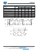
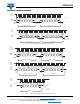
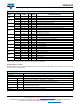
PARAMETER TIMING INFORMATION
Fig. 2 - I
2
C Bus Timing for Sending Word Command Format
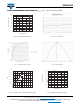
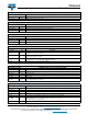
Fig. 3 - I
2
C Bus Timing for Receiving Word Command Format
W
SA6 SA5 SA4 SA3 SA2
SA1SA7
I2CBus Slave Address Byte
Start by
Master
ACK by
SA6 SA5 SA4 SA3 SA2
SA0
SA7
Command Code
SA1
ACK by
SA7
SA6 SA5 SA4 SA3 SA2 SA1
SA0
ACK by
SA7
SA6 SA5 SA4 SA3 SA2 SA1
SA0
Stop by
Master
ACK by
Data Byte Low Data Byte High
I
2
C bus
CLOCK
(SCLK)
I
2
C bus
DATA
(SDAT)
I
2
C bus
CLOCK
(SCLK)
I
2
C bus
DATA
(SDAT)
VCNL4040
VCNL4040
VCNL4040
VCNL4040
I2CBus
CLOCK
(SCLK)
I2CBus
DATA
(SDAT)
W
SA6 SA5 SA4 SA3 SA2
SA1SA7
I2CBus Slave Address Byte
Start by
Master
ACK by
SA6 SA5 SA4 SA3 SA2
SA0
SA7
Command Code
SA1
ACK by
SA7
SA6 SA5 SA4 SA3 SA2 SA1
SA0
Stop by
Master
ACK by
Master
Data Byte High
I2CBus
CLOCK
(SCLK)
I2CBus
DATA
(SDAT)
I2CBus
CLOCK
(SCLK)
I2CBus
DATA
(SDAT)
R
SA6 SA5 SA4 SA3 SA2
I2CBus Slave Address Byte
Start by
Master
ACK by
SA6 SA5 SA4 SA3 SA2
SA0
SA7
Data Byte Low
SA1
ACK by
Master
SA1
SA7
VCNL4040
VCNL4040
VCNL4040