
Data Sheet

VCNL4040
www.vishay.com
Vishay Semiconductors
Rev. 1.4, 02-Mar-15
16
Document Number: 84274
For technical questions, contact: sensorstechsupport@vishay.com
THIS DOCUMENT IS SUBJECT TO CHANGE WITHOUT NOTICE. THE PRODUCTS DESCRIBED HEREIN AND THIS DOCUMENT
ARE SUBJECT TO SPECIFIC DISCLAIMERS, SET FORTH AT www.vishay.com/doc?91000
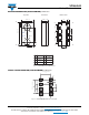
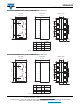
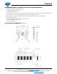
LAYOUT PAD INFORMATION (VCNL4040M3OE-H3, VCNL4040M3OE-H5) in millimeters
Fig. 18 - VCNL4040M3OE-H3 and H5 PCB Layout Footprint
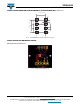
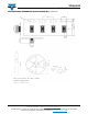
LAYOUT NOTICE AND REFERENCE CIRCUIT
Pad and Circuit Layout Reference
Fig. 19 - Suggested VCNL4040 Layout
Pad Center to Center
1.7
Pad Cente r to C
e
nter
0.725 x 8
0.9 x 8
1.075
0.45
0.8
1.075
1.075