
Data Sheet

VEML6075
www.vishay.com
Vishay Semiconductors
Rev. 1.2, 23-Nov-16
5
Document Number: 84304
For technical questions, contact: sensorstechsupport@vishay.com
THIS DOCUMENT IS SUBJECT TO CHANGE WITHOUT NOTICE. THE PRODUCTS DESCRIBED HEREIN AND THIS DOCUMENT
ARE SUBJECT TO SPECIFIC DISCLAIMERS, SET FORTH AT www.vishay.com/doc?91000
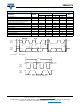
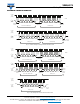
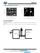
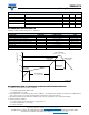
TYPICAL PERFORMANCE CHARACTERISTICS (T
amb
= 25 °C, unless otherwise specified)
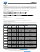
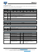
Fig. 4 - Normalized Spectral Response Fig. 5 - Normalized Output vs. View Angle
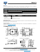
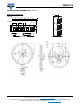
APPLICATION INFORMATION
Pin Connection with the Host
The configuration and data registers of the VEML6075 are accessed via the I
2
C interface. The hardware schematic is shown
below in fig. 6.
The 0.1 μF capacitor near the V
DD
pin is used for power supply noise rejection. The 2.2 kΩ is suitable for the pull high resistor
of I
2
C.
Fig. 6 - Hardware Pin Connection Diagram
10
100
1000
10000
0
10
20
30
40
50
60
70
80
90
100
300 350 400 450 500 550 600
Axis Title
1st line
2nd line
2nd line
Normalized Output (%)
λ - Wavelength (nm)
2nd line
UVB
UVA
UV
comp2
UV
comp1
0
10
20
30
40
50
60
70
80
90
100
-90 -60 -30 0 30 60 90
Axis Title
2nd line
Normalized Output (%)
Angle (deg)
2nd line
Cosine
UV-A
UV-B
10
100
1000
10000
1st line
2nd line
I
2
C bus data SDA
I
2
C bus clock SCL
SDA (2)
SCL (3)
GND (1)
V
DD
(4)
C1
100 nF
1.7 V to 3.6 V
1.7 V to 3.6 V
R2R1
Host
Micro Controller
VEML6075