
Data Sheet

VEML6075
www.vishay.com
Vishay Semiconductors
Rev. 1.2, 23-Nov-16
2
Document Number: 84304
For technical questions, contact: sensorstechsupport@vishay.com
THIS DOCUMENT IS SUBJECT TO CHANGE WITHOUT NOTICE. THE PRODUCTS DESCRIBED HEREIN AND THIS DOCUMENT
ARE SUBJECT TO SPECIFIC DISCLAIMERS, SET FORTH AT www.vishay.com/doc?91000
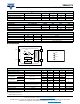
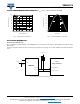
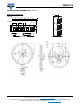
BLOCK DIAGRAM
Notes
(1)
Nichia NCSU033X (365 nm)
(2)
UVTOP310TO39HS (315 nm)
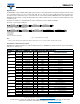
ABSOLUTE MAXIMUM RATINGS (T
amb
= 25 °C, unless otherwise specified)
PARAMETER TEST CONDITION SYMBOL MIN. MAX. UNIT
Supply voltage V
DD
03.6V
Operation temperature range T
amb
-40 +85 °C
Storage temperature range T
stg
-40 +85 °C
RECOMMENDED OPERATING CONDITIONS (T
amb
= 25 °C, unless otherwise specified)
PARAMETER TEST CONDITION SYMBOL MIN. MAX. UNIT
Supply voltage V
DD
1.7 3.6 V
Operation temperature range T
amb
-40 +85 °C
I
2
C bus operating frequency f
(I2CCLK)
10 400 kHz
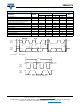
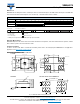
PIN DESCRIPTIONS
PIN ASSIGNMENT SYMBOL TYPE FUNCTION
1 GND I Ground
2 SDAT I / O (open drain) I
2
C data bus data input / output
3SCLKII
2
C digital bus clock input
4V
DD
I Power supply input
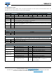
BASIC CHARACTERISTICS (T
amb
= 25 °C, unless otherwise specified)
PARAMETER TEST CONDITION SYMBOL MIN. TYP. MAX. UNIT
Supply operation voltage V
DD
1.7 - 3.6 V
Supply current V
DD
= 1.8 V I
DD
-480- μA
I
2
C signal input
Logic high
V
DD
= 3.3 V
V
IH
1.5 - -
V
Logic low V
IL
--0.8
I
2
C signal input
Logic high
V
DD
= 2.6 V
V
IH
1.4 - -
V
Logic low V
IL
--0.6
Operating temperature T
amb
-40 - +85 °C
Shutdown current
Light condition = dark;
V
DD
= 1.8 V, T
amb
= 25 °C
I
DD
(SD) - 800 - nA
UVA responsivity I
T
= 50 ms
(1)
- 0.93 - counts/μW/cm
2
UVB responsivity I
T
= 50 ms
(2)
- 2.1 - counts/μW/cm
2
Visible / infrared response W-LED / IRED (940 nm) - 0.5 < 1 %
V
DD
SCLSDA
GND
VEML6075
State machine
I
2
C interface
UV-PD
Oscillator
Timing
controller
V
DD
VEML6075 pin-out assignment
GND1
V
DD
4
SDAT2
SCLK3