
Data Sheet

AS7265x
Design Considerations
ams Application Note Page 9
[v1-5] 2018-May-23 Document Feedback
3.5 PCB Layout Considerations
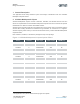
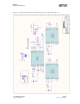
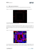
AS72651/AS72652/AS72653 has same 20-pin LGA package sharing same PCB footprint.
Figure 6. AS72651/AS72652/AS72653 PCB Footprint Recommendation
The schematic symbol and PCB layout footprint can also be provided in Altium Design format. Please
contact ams support team to get the library file.
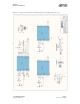
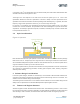
The PCB layout for AS72651/AS72652/AS72653 devices is simple. The first recommendation is to
place the decoupling capacitors closed to VDD pins of AS72651/AS72652/AS72653 devices. The
second recommendation is to avoid to put any via underneath the device. Please refer to the Figure
below.
Figure 7. Sample Layout of AS72651/AS72652/AS72653 Devices
For the system level layout consideration, the generic PCB layout rules for digital designs should
apply. In general, the wiring must be chosen so that crosstalk and interference to/from the bus lines