
Data Sheet

AH1815
Document number: DS37970 Rev. 2 - 2
3 of 13
www.diodes.com
September 2015
© Diodes Incorporated
AH1815
Absolute Maximum Ratings (Note 6) (@T
A
= +25°C, unless otherwise specified.)
Symbol
Parameter
Values
Unit
V
DD
Supply Voltage (Note 7)
7
V
V
OUT
Output Pin Voltage (Note 7)
7
V
V
DD REV
Reverse Supply Voltage
-0.3
V
V
OUT_REV
Reverse Output Pin Voltage
-0.3
V
I
OUTPUT
Output Current (Source and Sink)
2.5
mA
B
Magnetic Flux Density
Unlimited
P
D
Package Power Dissipation
SC59 and SOT553
230
mW
SIP-3
230
mW
T
STG
Storage Temperature Range
-65 to +150
°C
T
J
Maximum Junction Temperature
+150
°C
ESD HBM
Human Body Model ESD capability
6
kV
Notes: 6. Stresses greater than the 'Absolute Maximum Ratings' specified above may cause permanent damage to the device. These are stress ratings only;
functional operation of the device at these or any other conditions exceeding those indicated in this specification is not implied. Device reliability may
be affected by exposure to absolute maximum rating conditions for extended periods of time.
7. The absolute maximum V
DD
of 7V is a transient stress rating and is not meant as a functional operating condition. It is not recommended to operate
the device at the absolute maximum rated conditions for any period of time.
Recommended Operating Conditions (@T
A
= +25°C, unless otherwise specified.)
Symbol
Characteristic
Conditions
Rating
Unit
V
DD
Supply Voltage
Operating
2.5 to 5.5
V
V
OUT_MAX
Maximum Output Pin Voltage
Operating
5.5
V
T
A
Operating Temperature Range
Operating
-40 to +125
°C
Electrical Characteristics (@T
A
= +25°C, V
DD
= 3V, unless otherwise specified.)
Symbol
Characteristic
Conditions
Min
Typ
Max
Unit
V
OUT_ON
Output On Voltage
I
OUT
= 1mA
0.1
0.3
V
I
OFF
Output Leakage Current
V
OUT
= 5.5V, Output off
< 0.1
1
µA
I
DD
(Awake)
Supply Current
During awake period,
T
A
= +25°C, V
DD
= 3V
3
6
mA
During awake period,
T
A
= -40°C to +125°C, V
DD
= 2.5V to 5.5V
3
12
mA
I
DD
(Sleep)
During sleep period,
T
A
= +25°C, V
DD
= 3V
5
10
µA
I
DD
(Sleep)
During sleep period,
T
A
= -40°C to +125°C, V
DD
= 2.5V to 5.5V
28
µA
I
DD
(Avg.)
Average Supply Current
T
A
= +25°C, V
DD
= 3V
8
16
µA
T
A
= -40°C to +125°C, V
DD
= 2.5V to 5.5V
40
µA
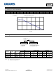
t
AWAKE
Awake Time
(Note 8)
75
125
µs
t
PERIOD
Period
(Note 8)
75
125
ms
D.C.
Duty Cycle
0.1
%
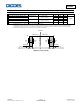
Note: 8. When power is initially turned on, the operating V
DD
must be within its correct operating range (2.5V to 5.5V) to guarantee the output sampling.
The output state is valid after the second operating cycle (typical 150ms).
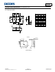
I
DD
(Sleep)
I
DD
(Awake)
t
AWAKE
t
PERIOD
0
Sample and output
latched
t
SLEEP
I
DD
(AVg.)