
Data Sheet

AH1815
Document number: DS37970 Rev. 2 - 2
2 of 13
www.diodes.com
September 2015
© Diodes Incorporated
AH1815
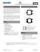
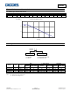
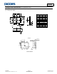
Typical Applications Circuit (Note 4)
AH1815
2.5V to 5.5V
OUTPUT
GND
R
L
C
IN
V
DD
Note: 4. C
IN
is for power stabilization and to strengthen the noise immunity, the recommended capacitance is 10nF to 100nF.
R
L
is the pull-up resistor, the recommended resistance is 10 to 100k.
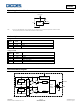
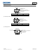
Pin Descriptions
Packages: SC59 and SIP-3
Pin
Number
Pin
Name
Function
1
V
DD
Power Supply Input
2
GND
Ground
3
OUTPUT
Output
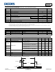
Package: SOT553
Pin
Number
Pin
Name
Function
1
NC
No Connection (Note 5)
2
GND
Ground
3
NC
No Connection (Note 5)
4
V
DD
Power Supply Input
5
OUTPUT
Output
Note: 5.
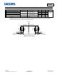
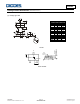
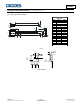
Functional Block Diagram
Output
Driver
Controller
Latch
Latch
Sleep/Awake Logic
and Power Switch
V
DD
Hall
Plate
Amp
Hall
Plate
Amp
Offset
Cancellation
Offset
Cancellation
OUTPUT
GND