
User Manual


Page 14 ams Datasheet
Document Feedback [v1-06] 2019-Feb-07
CCS811 − Application Information
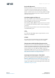
The recommended application circuit for CCS811 is shown
below.
Figure 11:
Recommended Application Circuit
Note(s):
1. The PWM (Pin 4) and Sense (Pin 5) signals on CCS811 must be connected together.
2. A decoupling capacitor must be placed close to the supply pin VDD on the CCS811.
3. The value of the pull-ups for SCL and SDA depends on the host system configuration (desired bus speed, bus length, number of
slaves, etc.).
4. If power is not an issue, nWake can be connected to ground if a spare GPIO is not available on the host processor.
5. ADDR must be connected to either VDD (logic 1) or ground (logic 0) depending on the required lsb of the CCS811’s I²C slave address.
Host System Software Requirements
1. The minimum level of driver support that a host system
needs is read and write I²C transactions of data bytes
where the nWAKE pin is asserted at least tAWAKE before
the transaction and kept asserted throughout.
2. An Interrupt handler is also recommended to tell the
application code that the device has asserted an
interrupt.
Application Information
Host
Processor
V
DD
R
SDA
SCL
V
DD
GND
CCS811
Digital VOC sensor
4k7
4.7μF
GPIOx
SDA
ADDR
SCL
nWAKE
PWM
Sense
nReset
Reset
R
nINT
Interrupt
4k7