CCS811 Ultra-Low Power Digital Gas Sensor for Monitoring Indoor Air Quality General Description The CCS811 is an ultra-low power digital gas sensor solution which integrates a metal oxide (MOX) gas sensor to detect a wide range of Volatile Organic Compounds (VOCs) for indoor air quality monitoring with a microcontroller unit (MCU), which includes an Analog-to-Digital converter (ADC), and an I²C interface.
CCS811 − General Description Key Benefits & Features The benefits and features of CCS811, Ultra-Low Power Digital Gas Sensor for Monitoring Indoor Air Quality are listed below: Figure 1: Added Value of Using CCS811 Sensor Benefits Features • Manages the sensor drive modes and measurements while detecting VOCs • Integrated MCU • Provides eCO2 level or eTVOC indication with no host intervention • On-board processing • Simplifies the hardware and software integration • Standard (100kbit/s) and fast (4
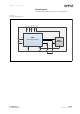
CCS811 − General Description Block Diagram The functional blocks of this device are shown below: Figure 2: CCS811 Block Diagram 10 6 VDD SCL 9 SDA 1 ADDR 8 H+ (With Integrated ADC) nRESET 7 EP Sense PWM GND H- nWAKE 2 MCU nINT 3 S+ 4 MOX Gas Sensor S- 5 Pins 4 and 5 mu st be connected together ams Datasheet [v1-06] 2019-Feb-07 Page 3 Document Feedback
CCS811 − Pin Assignment Pin Assignment Figure 3: Pin Diagram Pin 1 Corner Index Area (Top View) (Bottom View) 5 6 4 7 8 3 2 9 1 10 Pin 1 Corner Index Area Pin Diagram: The Exposed Pad is underneath Figure 4: CCS811 LGA Pin Assignment Pin No. Pin Name 1 ADDR Description Single address select bit to allow alternate address to be selected • When ADDR is low the 7 bit I²C address is decimal 90 / hex 0x5A • When ADDR is high the 7 bit I²C address is decimal 91 / hex 0x5B.
CCS811 − Absolute Maximum Ratings Absolute Maximum Ratings Stresses beyond those listed under Absolute Maximum Ratings may cause permanent damage to the device. These are stress ratings only. Functional operation of the device at these or any other conditions beyond those indicated under Electrical Characteristics is not implied.
CCS811 − Electrical Characteristics Electrical Characteristics Figure 6: Electrical Characteristics Parameters Conditions Min Supply Voltage (VDD) (1), (2) Supply Current (IDD) (3) Typ (6) 1.8 Max Units 3.3 V During measuring at 1.8V 26 mA Average over pulse cycle(3) at 1.8V 0.7 mA Sleep Mode at 1.8V 19 μA Idle Mode 0 at VDD= 1.8V 0.034 mW Mode 1 & 4 at VDD= 1.8V 46 mW Mode 2 at VDD= 1.8V 7 mW Mode 3 at VDD= 1.8V 1.
CCS811 − Electrical Characteristics Figure 7: Timing Characteristics Parameters Conditions tAPP_START tWAKE (1) Min Typ Max Units Time between giving the APP_START command in boot mode and the device being ready for new I²C commands 1 ms Time after falling nWAKE and the device being ready for new I2C commands 50 μs Time between power on and the device being ready for new I²C commands 18 20 ms Time after rising nRESET pin or giving the SW_RESET command and the device being ready for new I
CCS811 − Electrical Characteristics Figure 8: CCS811 Timings SCL/SDA tSTART Min delay of 20ms till start of I²C APP_START tAPP_START Min delay of 1ms till start of I²C Application Commands VDD tSTART Min delay of 2ms till start of I²C SCL/SDA nRESET tRESET Min length of 15μs for reset pulse SCL/SDA tWAKE Min delay of 50μs till start of I²C nWAKE Page 8 Document Feedback Commands tDRESET Min high time of 20μs after reset Commands Commands tDW AKE Min high time of 20μs after wake ams Datas
CCS811 − Detailed Description Detailed Description State Machine The state machine for CCS811 is shown below: Figure 9: CCS811 State Machine nRESET pulsed Off power on power off On Boot APP_ERASE APP_DATA APP_VERIFY SW_RESET App Idle mode=0 Idle Erasing mode=1 Mode1s Writing mode=2 Mode10s Verifying mode=3 Mode60s mode=4 Mode.25s APP_START When powering on the CCS811, a typical action is to transition from Boot to App mode, a write to register APP_START with no data is required.
CCS811 − Detailed Description Power States The previous diagram showed that when the CCS811 is powered On it can be in several functional states (e.g. App with Mode1s). Orthogonal to this, when the CCS811 is On, it can be in several power states. The diagram below illustrates the power behavior.
CCS811 − Detailed Description Note that a hardware reset (via the nRESET) pin can be triggered irrespective of the power state (assuming On), for a SW_RESET, the CCS811 needs to be Wake. So, tying nWAKE to ground is the simplest hardware configuration – CCS811 will always be Wake and ready to communicate but consumes more power. If power consumption is a concern, the master should set nWAKE low before I2C communication and high afterwards.
CCS811 − Detailed Description Early-Life (Burn-In) CCS811 performance in terms of resistance levels and sensitivities will change during early life. The change in resistance is greatest over the first 48 hours of operation. CCS811 controls the burn-in period allowing eCO 2 and eTVOC readings to be used from first power-on after 60 minutes of operation in modes 1-3.
CCS811 − Detailed Description Automatic Baseline Correction The resistance R S of the sensitive layer is the output of the sensor. However, metal oxide sensors do not give absolute readings. The resistance R S varies from sensor to sensor (manufacturing variation), from use-case to use-case, and over time. To mitigate this problem, the output of the sensor is normalized: R S is divided by R A. The value of R A is known as the baseline.
CCS811 − Application Information The recommended application circuit for CCS811 is shown below. Application Information Figure 11: Recommended Application Circuit VDD R Host Processor R 4k7 VDD 4k7 CCS811 Digital VOC sensor SCL SCL SDA SDA 4.7μF GPIOx nWAKE Reset nReset Interrupt PWM nINT Sense ADDR GND Note(s): 1. The PWM (Pin 4) and Sense (Pin 5) signals on CCS811 must be connected together. 2. A decoupling capacitor must be placed close to the supply pin VDD on the CCS811. 3.
CCS811 − Application Information I²C Interface I²C transactions require a register address to be selected (written) and followed by data, as described by the transaction types in the subsections below. Each Register location corresponds to a byte or multiple bytes. Multiple reads or writes in a single sequence will be to or from the same location (the address does not increment). Therefore, registers are sometimes referred to as mailboxes in this document.
CCS811 − Application Information I²C Register Read Figure 13: I²C Register Read Select and read register value Select and read register value, as single transaction Select and repeatedly read multiple data values from register S SLAVE ADDRESS W A DATA(REG ADDR) A P (select register address) S SLAVE ADDRESS R A DATA N P (read register value) S SLAVE ADDRESS W A DATA(REG ADDR) A S SLAVE ADDRESS (select register address) R A DATA N P (read register value) A P (select register addre
CCS811 − Application Register Overview Application Register Overview All I²C transactions must use the (7 bits) slave address 0x5A or 0x5B depending on status of ADDR pin when writing to and reading from the CCS811. Figure 14 shows the register map for CCS811. Figure 25 shows the bootloader register map.
CCS811 − Application Register Overview STATUS Register (0x00) Single byte read only register which indicates if a device is active, if new data is available or if an error occurred. Figure 15: Status Register 7 6 5 4 3 FW_MODE APP_ERASE APP_VERIFY APP_VALID DATA_READY Bit(s) Field 7 FW_MODE 0: Firmware is in boot mode, this allows new firmware to be loaded 1: Firmware is in application mode. CCS811 is ready to take ADC measurements APP_ERASE Boot Mode only.
CCS811 − Application Register Overview MEAS_MODE (Measurement and Conditions) Register (0x01) This is Single byte register, which is used to enable sensor drive mode and interrupts.
CCS811 − Application Register Overview ALG_RESULT_DATA (Algorithm Results Data) Register (0x02) This multi-byte read only register contains the calculated eCO2 (ppm) and eTVOC (ppb) values followed by the STATUS register, ERROR_ID register and the RAW_DATA register. • If only eCO 2 is required, only the first 2 bytes need to be read. • If eTVOC is required, 4 bytes need to be read.
CCS811 − Application Register Overview ENV_DATA (Environment Data) Register (0x05) A multi-byte register that can be written with the current Humidity and Temperature values if known.
CCS811 − Application Register Overview THRESHOLDS Register (0x10) If ‘interrupt on threshold change’ has been set in the Mode register (see above), the values in this multi- byte write only register are used to determine the thresholds.
CCS811 − Application Register Overview FW_Boot_Version (Firmware Bootloader Version) Register (0x23) Two byte read only register which contain the version of the firmware bootloader stored in the CCS811 in the format Major.Minor.
CCS811 − Application Register Overview ERROR_ID (Error Identifier) Register (0xE0) If the ERR bit [0] of the STATUS Register is set, this single byte read only register indicates source(s) of the error.
CCS811 − Application Register Overview SW_RESET Register (0xFF) As an alternative to Power-On reset or Hardware Reset a Software Reset is available. Asserting the SW_RESET will restart the CCS811 in Boot mode to enable new application firmware to be downloaded. To prevent accidental SW_RESET a sequence of four bytes must be written to this register in a single I²C sequence: 0x11, 0xE5, 0x72, 0x8A. For details, please refer to application notes ams AN000369 and ams AN000371.
CCS811 − Bootloader Register Over view Bootloader Register Overview All I²C transactions must use the (7bits) slave address 0x5A or 0x5B depending on status of ADDR pin when writing to and reading from the CCS811. Figure 25 shows the bootloader register map for CCS811. Figure 25: CCS811 Bootloader Register Map Address Register R/W Size Description 0x00 STATUS R 1 byte Status register 0x20 HW_ID R 1 byte Hardware ID. The value is 0x81 0x21 HW Version R 1 byte Hardware Version.
CCS811 − Bootloader Register Overview Registers not detailed below are documented in the Application Register Overview section. APP_ERASE (Application Erase) Register (0xF1) To prevent accidental APP_ERASE a sequence of four bytes must be written to this register in a single I²C sequence: 0xE7, 0xA7, 0xE6, 0x09. The APP_ERASE can take a variable amount of time. The status register can be polled to determine when this function is complete.
CCS811 − Package Drawings & Mark ing Package Drawings & Marking LGA Package Outline Figure 26: LGA Package Drawings Pin 1 Corner Index Area (Top View) (Side View) D A E 1.2 nxL nxW 6 5 e D1 2.4 1 Pin 1 Corner Index Area RoHS 10 (0.3) Green E1 (Bottom View) Symbol Total thickness Body Size Lead Width Lead Length Lead Pitch Lead Count Edge Lead Centre to Centre A D E W L e n D1 E1 Min - 0.25 0.45 Dimensions Nominal 4.0 2.7 0.3 0.5 0.6 10 2.4 2.2 Max 1.1 BSC BSC 0.35 0.
CCS811 − Package Drawings & Marking The recommended package footprint or landing pattern for CCS811 is shown below: Figure 27: Recommended Package Footprint for CCS811 2.7 0.6 0.3 0.75 1 10 0.3 0.4 0.6 4 0.4 5 6 1.3 0.7 (Top View) Note(s): 1. All dimensions are in millimeters. 2. PCB land pattern in Green dash lines 3. Pin numbers are in Red 4. Add 0.
CCS811 − Ordering & Contact Information Ordering & Contact Information Figure 28: Ordering Information Ordering Code Description Package MOQ CCS811B-JOPR5K CCS811 digital gas sensor for Indoor Air Quality Monitoring 2.7mm x 4.0mm x 1.1mm LGA 5000 CCS811B-JOPD500 CCS811 digital gas sensor for Indoor Air Quality Monitoring 2.7mm x 4.0mm x 1.1mm LGA 500 Note(s): 1. Refer to JEDEC J-STD020 lead-free standard for typical soldering reflow profile Technical Support is available at: www.ams.
CCS811 − RoHS Compliant & ams Green Statement RoHS Compliant & ams Green Statement RoHS: The term RoHS compliant means that ams AG products fully comply with current RoHS directives. Our semiconductor products do not contain any chemicals for all 6 substance categories, including the requirement that lead not exceed 0.1% by weight in homogeneous materials. Where designed to be soldered at high temperatures, RoHS compliant products are suitable for use in specified lead-free processes.
CCS811 − Copyrights & Disclaimer Copyrights & Disclaimer Copyright ams AG, Tobelbader Strasse 30, 8141 Premstaetten, Austria-Europe. Trademarks Registered. All rights reserved. The material herein may not be reproduced, adapted, merged, translated, stored, or used without the prior written consent of the copyright owner. Devices sold by ams AG are covered by the warranty and patent indemnification provisions appearing in its General Terms of Trade.
CCS811 − Document Status Document Status Document Status Product Preview Preliminary Datasheet Datasheet Datasheet (discontinued) ams Datasheet [v1-06] 2019-Feb-07 Product Status Definition Pre-Development Information in this datasheet is based on product ideas in the planning phase of development.
CCS811 − Revision Information Revision Information Changes from 1-05 (2018-May-01) to current revision 1-06 (2019-Feb-07) Page Updated figure 6 6 Updated figure 7 7 Added figure 8 8 Added “State Machine” under “Detailed Description” 9 Added “Power States” under “Detailed Description” 10 Updated and Renamed “Early-Life Use (Burn-In)” to “Early-Life (Burn-In)” 12 Updated Conditioning Period (Run-In), eCO2, Temperature and Humidity Compensation 12 Updated figure 11 and notes under it 14 Upd
CCS811 − Appendix Appendix References Figure 29: Document Reference Document Reference Description ams AN000367 CCS811 Assembly guidelines ams AN000368 CCS811 Design guidelines ams AN000369 CCS811 Programming and interfacing guide ams AN000370 CCS811 Clean air baseline save and restore ams AN000371 CCS811 Performing a firmware download ams AN000373 CCS811 Factory test procedure ams Datasheet [v1-06] 2019-Feb-07 Page 35 Document Feedback
CCS811 − Content Guide Content Guide 1 2 2 3 General Description Key Benefits & Features Applications Block Diagram 4 5 6 Pin Assignment Absolute Maximum Ratings Electrical Characteristics 9 9 10 11 11 12 12 12 12 12 13 13 Detailed Description State Machine Power States Modes of Operation Early-Life (Burn-In) Conditioning Period (Run-In) eCO2 eTVOC Temperature and Humidity Compensation Interrupt and Interrupt on Threshold Automatic Baseline Correction Manual Baseline Correction 14 14 15 15 16 Appli
CCS811 − Content Guide ams Datasheet [v1-06] 2019-Feb-07 28 28 Package Drawings & Marking LGA Package Outline 30 31 32 33 34 Ordering & Contact Information RoHS Compliant & ams Green Statement Copyrights & Disclaimer Document Status Revision Information 35 35 Appendix References Page 37 Document Feedback