
Data Sheet


bq24072
,
bq24073
,
bq24074
,
bq24075
,
bq24079
SLUS810K –SEPTEMBER 2008–REVISED MARCH 2015
www.ti.com
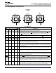
Pin Functions (continued)
PIN
I/O DESCRIPTION
NAME '72, '73 '74 '75, '79
There is an internal electrical connection between the exposed thermal pad and the VSS pin of the device.
Thermal The thermal pad must be connected to the same potential as the VSS pin on the printed circuit board. Do not
— — — –
Pad use the thermal pad as the primary ground input for the device. VSS pin must be connected to ground at all
times.
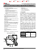
Timer Programming Input. TMR controls the pre-charge and fast-charge safety timers. Connect TMR to VSS
TMR 14 14 14 I to disable all safety timers. Connect a 18-kΩ to 72-kΩ resistor between TMR and VSS to program the timers
a desired length. Leave TMR unconnected to set the timers to the default values.
External NTC Thermistor Input. Connect the TS input to the NTC thermistor in the battery pack. TS monitors
TS 1 1 1 I a 10kΩ NTC thermistor. For applications that do not use the TS function, connect a 10-kΩ fixed resistor from
TS to VSS to maintain a valid voltage level on TS.
VSS 8 8 8 – Ground. Connect to the thermal pad and to the ground rail of the circuit.
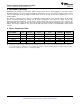
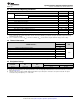
EN1/EN2 Settings
EN2 EN1 MAXIMUM INPUT CURRENT INTO IN PIN
0 0 100 mA. USB100 mode
0 1 500 mA. USB500 mode
1 0 Set by an external resistor from ILIM to VSS
1 1 Standby (USB suspend mode)
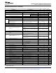
8 Specifications
8.1 Absolute Maximum Ratings
(1)
over the 0°C to 125°C operating free-air temperature range (unless otherwise noted)
MIN MAX UNIT
IN (with respect to VSS) –0.3 28 V
BAT (with respect to VSS) –0.3 5 V
V
I
Input Voltage
OUT, EN1, EN2, CE, TS, ISET, PGOOD, CHG, ILIM,
–0.3 7 V
TMR, ITERM, SYSOFF, TD (with respect to VSS)
I
I
Input Current IN 1.6 A
OUT 5 A
Output Current
I
O
BAT (Discharge mode) 5 A
(Continuous)
BAT (Charging mode) 1.5
(2)
A
Output Sink Current CHG, PGOOD 15 mA
T
J
Junction temperature –40 150 °C
T
stg
Storage temperature –65 150 °C
(1) Stresses beyond those listed under Absolute Maximum Ratings may cause permanent damage to the device. These are stress ratings
only, and functional operation of the device at these or any other conditions beyond those indicated under Recommended Operating
Conditions is not implied. Exposure to absolute-maximum-rated conditions for extended periods may affect device reliability. All voltage
values are with respect to the network ground terminal unless otherwise noted.
(2) The IC operational charging life is reduced to 20,000 hours, when charging at 1.5A and 125°C. The thermal regulation feature reduces
charge current if the IC’s junction temperature reaches 125°C; thus without a good thermal design the maximum programmed charge
current may not be reached.
8.2 ESD Ratings
VALUE UNIT
Human body model (HBM), per ANSI/ESDA/JEDEC JS-001
(1)
±2000
V
(ESD)
Electrostatic discharge V
Charged-device model (CDM), per JEDEC specification JESD22- ±500
C101
(2)
(1) JEDEC document JEP155 states that 500-V HBM allows safe manufacturing with a standard ESD control process.
(2) JEDEC document JEP157 states that 250-V CDM allows safe manufacturing with a standard ESD control process.
6 Submit Documentation Feedback Copyright © 2008–2015, Texas Instruments Incorporated
Product Folder Links: bq24072 bq24073 bq24074 bq24075 bq24079