
Data Sheet


1
2
3
4
12
11
10
9
ILIM
OUT
OUT
CHG
TS
BAT
BAT
CE
ISET
TD
PGOOD
VSS
TMR
IN
EN2
EN1
16 15 14 13
5 6 7 8
bq24075
bq24079
1
2
3
4
12
11
10
9
ILIM
OUT
OUT
CHG
TS
BAT
BAT
CE
ISET
ITERM
PGOOD
VSS
TMR
IN
EN2
EN1
16 15 14 13
5 6 7 8
bq24074
SYSOFF
1
2
3
4
12
11
10
9
ILIM
OUT
OUT
CHG
TS
BAT
BAT
CE
ISET
PGOOD
VSS
TMR
IN
EN2
EN1
16 15 14 13
5 6 7 8
bq24072
bq24073
bq24072
,
bq24073
,
bq24074
,
bq24075
,
bq24079
www.ti.com
SLUS810K –SEPTEMBER 2008–REVISED MARCH 2015
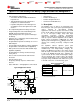
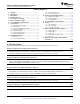
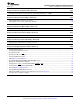
7 Pin Configuration and Functions
RGT Package
16 Pins
Top View
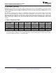
Pin Functions
PIN
I/O DESCRIPTION
NAME '72, '73 '74 '75, '79
Charger Power Stage Output and Battery Voltage Sense Input. Connect BAT to the positive terminal of the
BAT 2, 3 2, 3 2, 3 I/O
battery. Bypass BAT to VSS with a 4.7-μF to 47-μF ceramic capacitor.
Charge Enable Active-Low Input. Connect CE to a high logic level to place the battery charger in standby
mode. In standby mode, OUT is active and battery supplement mode is still available. Connect CE to a low
CE 4 4 4 I
logic level to enable the battery charger. CE is internally pulled down with approximately 285 kΩ. Do not
leave CE unconnected to ensure proper operation.
Open-Drain Charging Status Indication Output. CHG pulls to VSS when the battery is charging. CHG is high
CHG 9 9 9 O impedance when charging is complete and when charger is disabled. Connect CHG to the desired logic
voltage rail using a 1kΩ-100kΩ resistor, or use with an LED for visual indication.
EN1 6 6 6 I Input Current Limit Configuration Inputs. Use EN1 and EN2 control the maximum input current and enable
USB compliance. See Table 2 for the description of the operation states. EN1 and EN2 are internally pulled
EN2 5 5 5 I
down with ≉285 kΩ. Do not leave EN1 or EN2 unconnected to ensure proper operation.
Adjustable Current Limit Programming Input. Connect a 1100-Ω to 8-kΩ resistor from ILIM to VSS to program
ILIM 12 12 12 I the maximum input current (EN2=1, EN1=0). The input current includes the system load and the battery
charge current. Leaving ILIM unconnected disables all charging.
Input Power Connection. Connect IN to the external DC supply (AC adapter or USB port). The input operating
range is 4.35 V to 6.6 V (bq24072, bq24073, bq24075, and bq24079) or 4.35 V to 10.5 V (bq23074). The
IN 13 13 13 I
input can accept voltages up to 26 V without damage but operation is suspended. Connect bypass capacitor
1 μF to 10 μF to VSS.
Fast Charge Current Programming Input. Connect a 590-Ω to 8.9-kΩ resistor from ISET to VSS to program
the fast charge current level. Charging is disabled if ISET is left unconnected. While charging, the voltage at
ISET 16 16 16 I/O
ISET reflects the actual charging current and can be used to monitor charge current. See Charge Current
Translator for more details.
Termination Current Programming Input. Connect a 0-Ω to 15-kΩ resistor from ITERM to VSS to program the
ITERM – 15 – I termination current. Leave ITERM unconnected to set the termination current to the default 10% termination
threshold.
System Supply Output. OUT provides a regulated output when the input is below the OVP threshold and
above the regulation voltage. When the input is out of the operation range, OUT is connected to V
BAT
except
OUT 10, 11 10, 11 10, 11 O
when SYSOFF is high (bq24075 and bq24079 only). Connect OUT to the system load. Bypass OUT to VSS
with a 4.7-μF to 47-μF ceramic capacitor.
Open-drain Power Good Status Indication Output. PGOOD pulls to VSS when a valid input source is
PGOOD 7 7 7 O detected. PGOOD is high-impedance when the input power is not within specified limits. Connect PGOOD to
the desired logic voltage rail using a 1-kΩ to 100-kΩ resistor, or use with an LED for visual indication.
System Enable Input. Connect SYSOFF high to turn off the FET connecting the battery to the system output.
When an adapter is connected, charging is also disabled. Connect SYSOFF low for normal operation.
SYSOFF – – 15 I
SYSOFF is internally pulled up to V
BAT
through a large resistor (approximately 5 MΩ). Do not leave SYSOFF
unconnected to ensure proper operation.
Termination Disable Input. Connect TD high to disable charger termination. Connect TD to VSS to enable
charger termination. TD is checked during startup only and cannot be changed during operation. See the TD
TD 15 – – I
section in this datasheet for a description of the behavior when termination is disabled. TD is internally pulled
down to VSS with approximately 285 kΩ. Do not leave TD unconnected to ensure proper operation.
Copyright © 2008–2015, Texas Instruments Incorporated Submit Documentation Feedback 5
Product Folder Links: bq24072 bq24073 bq24074 bq24075 bq24079