
Data Sheet

bq27441-G1
www.ti.com
SLUSBH1C –NOVEMBER 2013–REVISED DECEMBER 2014
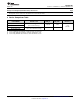
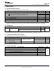
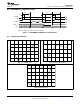
8.7 LDO Regulator, Wake-up, and Auto-Shutdown DC Characteristics
T
A
= –40°C to 85°C, typical values at T
A
= 30°C and V
REGIN
= 3.6 V (unless otherwise noted)(Force Note1)
(1)
PARAMETER TEST CONDITIONS MIN TYP MAX UNIT
V
BAT
BAT pin regulator input 2.45 4.5 V
V
DD
Regulator output voltage 1.8 V
V
BAT
undervoltage lock-out
UVLO
IT+
2 V
LDO wake-up rising threshold
V
BAT
undervoltage lock-out
UVLO
IT–
1.95 V
LDO auto-shutdown falling threshold
GPOUT (input) LDO Wake-up rising LDO Wake-up from SHUTDOWN
V
WU+
(1)
1.2 V
edge threshold
(2)
mode
(1) Specified by design. Not production tested.
(2) If the device is commanded to SHUTDOWN via I
2
C with V
BAT
> UVLO
IT+
, a wake-up rising edge trigger is required on GPOUT.
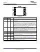
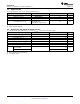
8.8 LDO Regulator, Wake-up, and Auto-shutdown AC Characteristics
T
A
= –40°C to 85°C, typical values at T
A
= 30°C and V
REGIN
= 3.6 V (unless otherwise noted)
PARAMETER TEST CONDITIONS MIN TYP MAX UNIT
Time delay from SHUTDOWN
t
SHDN
(1)
SHUTDOWN entry time 250 ms
command to LDO output disable.
Minimum low time of GPOUT (input)
t
SHUP
(1)
SHUTDOWN GPOUT low time 10 μs
in SHUTDOWN before WAKEUP
t
VDD
(1)
Initial V
DD
output delay 13 ms
Time delay from rising edge of
t
WUVDD
(1)
Wake-up V
DD
output delay GPOUT (input) to nominal V
DD
8 ms
output.
Time delay from rising edge of
t
PUCD
Power-up communication delay REGIN to the Active state. Includes 250 ms
firmware initialization time.
(1) Specified by design. Not production tested.
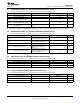
8.9 ADC (Temperature and Cell Measurement) Characteristics
T
A
= –40°C to 85°C; typical values at T
A
= 30°C and V
REGIN
= 3.6 V (unless otherwise noted) (Force Note1)
(1)
PARAMETER TEST CONDITIONS MIN TYP MAX UNIT
V
IN(BAT)
BAT pin voltage measurement range Voltage divider enabled 2.45 4.5 V
t
ADC_CONV
Conversion time 125 ms
Effective resolution 15 bits
(1) Specified by design. Not tested in production.
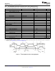
8.10 Integrating ADC (Coulomb Counter) Characteristics
T
A
= –40°C to 85°C; typical values at T
A
= 30°C and V
REGIN
= 3.6 V (unless otherwise noted)(Force Note1)
(1)
PARAMETER TEST CONDITIONS MIN TYP MAX UNIT
V
SR
Input voltage range from BAT to BAT ± 25 mV
SRX pins
t
SR_CONV
Conversion time Single conversion 1 s
Effective Resolution Single conversion 16 bits
(1) Specified by design. Not tested in production.
Copyright © 2013–2014, Texas Instruments Incorporated Submit Documentation Feedback 7
Product Folder Links: bq27441-G1