
Data Sheet

bq27441-G1
www.ti.com
SLUSBH1C –NOVEMBER 2013–REVISED DECEMBER 2014
8 Specifications
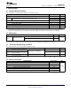
8.1 Absolute Maximum Ratings
over operating free-air temperature range (unless otherwise noted)
(1)
MIN MAX UNIT
V
BAT
BAT pin input voltage range –0.3 6 V
SRP and SRN pins input voltage range –0.3 V
BAT
+ 0.3 V
V
SR
Differential voltage across SRP and SRN. ABS(SRP – SRN) 2 V
V
DD
V
DD
pin supply voltage range (LDO output) –0.3 2 V
V
IOD
Open-drain IO pins (SDA, SCL) –0.3 6 V
V
IOPP
Push-pull IO pins (BIN) –0.3 V
DD
+ 0.3 V
T
A
Operating free-air temperature range –40 85 °C
Storage temperature, T
stg
–65 150 °C
(1) Stresses beyond those listed under "absolute maximum ratings" may cause permanent damage to the device. These are stress ratings
only, and functional operation of the device at these or any other conditions beyond those indicated under "recommended operating
conditions" is not implied. Exposure to absolute-maximum-rated conditions for extended periods may affect device reliability.
8.2 ESD Ratings
VALUE UNIT
Human body model (HBM), per ANSI/ESDA/JEDEC JS-001
(1)
±1500
V
(ESD)
Electrostatic discharge V
Charged-device model (CDM), per JEDEC specification JESD22-
±250
C101
(2)
(1) JEDEC document JEP155 states that 500-V HBM allows safe manufacturing with a standard ESD control process.
(2) JEDEC document JEP157 states that 250-V CDM allows safe manufacturing with a standard ESD control process.
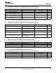
8.3 Recommended Operating Conditions
T
A
= 30°C and V
REGIN
= V
BAT
= 3.6 V (unless otherwise noted)
MIN TYP MAX UNIT
External input capacitor for internal LDO
C
BAT
(1)
0.1 μF
Nominal capacitor values specified.
between BAT and V
SS
Recommend a 5% ceramic X5R-type
External output capacitor for internal LDO
capacitor located close to the device.
C
LDO18
(1)
0.47 μF
between V
DD
and V
SS
External pullup voltage for open-drain
V
PU
(1)
1.62 3.6 V
pins (SDA, SCL, GPOUT)
(1) Specified by design. Not production tested.
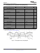
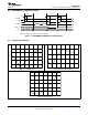
8.4 Thermal Information
THERMAL METRIC DRZ (12 PINS) UNIT
R
θJA
Junction-to-ambient thermal resistance 64.1
R
θJCtop
Junction-to-case (top) thermal resistance 59.8
R
θJB
Junction-to-board thermal resistance 52.7
°C/W
ψ
JT
Junction-to-top characterization parameter 0.3
ψ
JB
Junction-to-board characterization parameter 28.3
R
θJCbot
Junction-to-case (bottom) thermal resistance 2.4
Copyright © 2013–2014, Texas Instruments Incorporated Submit Documentation Feedback 5
Product Folder Links: bq27441-G1