
User Manual

Page 85
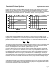
A: Difficult to say, before we optimize many of the variables, but 0.2 to 0.5 Mr. & Mrs. steps look practical
right now. So 1.0, 1.5 and 2.0 Mr. & Mrs. walls would certainly work – if necessary, the imbalance in internal
volume could be made up by adding or subtracting material elsewhere in the chamber. The step size could
be smaller, if we push for “perfect” ultrasonic waveform and possibly higher frequency.
Q: My cartridges have sponges inside. Will this affect the performance?
A: We believe not. It seems so far that a dry sponge looks just like air, and a wet sponge just like ink. It
really is quite difficult to get good ultrasonic coupling at 20 MHZ frequency, and the dry sponge simply lying in
contact with the wall does not, as far as we can tell, absorb any of the ultrasonic energy at the interface. Even
pushing a solid, flat block of polymer against the inside wall doesn’t affect the signal unless a significant
amount of force is applied, or liquid is allowed to penetrate into the gap.
Q: It sounds like the fixing of the sensor onto the wall is going to be quite a challenge!
A: The ideal case would be a very thin layer of liquid adhesive, which then cured to reach a hard state –
epoxy works great! But we appreciate that a liquid process may not prove acceptable in production. We
may be able to procure an off-the-shelf “transfer adhesive” (in tape form) which we can laminate to our film
during our production cycle. Alternatively, we may need to enter into a dialog with a tape converter who
could develop and apply a coating (with release liner) onto our film.
We envisage supplying reels of self-adhesive “labels”, kiss-cut to allow easy application onto cartridges.
Q: I understand the principle of the sensor. Now, how do we connect to this “label”?
A: We’re working on this! One possibility is lightly-sprung contacts, which would be brought into contact
only when the cartridge is at rest. Our electrode surface will be either sputtered metallization (around 500
a
thick) or printed silver ink (about 7 µm), so we don’t think a wiping contact would be appropriate. Another
possibility is capacitive coupling, if we can arrange some reasonable area of electrode surface (for both
signal and ground tracks) to come into proximity with a similar arrangement fixed to the printer. There would
be further signal losses, and probably additional tolerance variations, if this method were adopted. This is
partly a cost issue – if we add too much area to the sensor just for capacitive coupling, the cost of this
inactive area may jeopardize the economics of the whole solution.
The connection scheme also has to take into account the physical layout and practicalities of the printer
itself. We can’t design the solution in a vacuum – we need input from both the mechanical and electronic
design teams responsible for the printer.
Q: Where should the interface electronics be located? Can I integrate these into an ASIC on the
main pcb?
A: We think so. The sensor will be designed to have as low an impedance as practical at the operating
frequency – ideally 50 ohms. Although we have, in theory, a small “antenna” connected to the gain stage, in
practice we don’t see noise pick-up as being a major problem. Shielded cable, or “gnd-sig-gnd” coplanar
wiring would be preferred for carrying the signals over any significant distance within the printer. Our
measurement process should only take a few microseconds, so it is possible that a “quiet time” (as far as
intentional digital or control activity is concerned) could be selected to make the measurement. Noise
radiation and immunity would need to be considered and reviewed throughout the design process.
Q: What control do I have over the “switching point”?
A: The placement of the sensor, of course, dictates the basic depth of ink where the “switch” will change
state. Ideally, the active electrode area would be a narrow horizontal line. In practice, we prefer to use a
rectangular element to increase the capacitance of the sensor (which allows better matching to practical
electronics). The “switching point” will nominally occur at the vertical midpoint of the sensor. A “height” in
the region of 5 to 10 Mr. & Mrs. appears likely for the overall “label”, so the lowest sensing depth may be 2.5
to 5.0 Mr. & Mrs. Temperature effects may vary the apparent location of this switching point, but worst-case
uncertainty would be determined by the active electrode height.
Q: What factors would MSI wish to influence in my cartridge design?
A: The base material has an influence on the effectiveness of the solution. Some polymers (such as
Nylon and acetyl) have high attenuation in the ultrasonic region. A close match of acoustic impedance