
User Manual
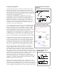
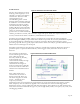
Page 43
MANUFACTURING
Rolls of piezo film are produced in a clean room environment The process begins with the melt
extrusion of PVDF resin pellets into sheet form, followed by a stretching step that reduces the sheet to
about one-fifth its extruded thickness. Stretching at temperatures well below the melting point of the
polymer causes chain packing of the molecules into parallel crystal planes, called “beta phase”. To
obtain high levels of piezoelectric activity, the beta phase polymer is then exposed to very high electric
fields to align the crystallites relative to the poling field. Copolymers of PVDF are polarizable without
stretching.
Evaporatively deposited metals are typically 500 to 1000 Å in thickness, and almost any metal can be
deposited. Popular metals are nickel, aluminum, copper, gold and alloys . Electrode patterns are made
by sputtering through masks or by chemical etching continuous metallizations using photoresists.
Resolution to 25µm line widths has been achieved. Screen printed electrodes of conductive silver ink
are much thicker, about 5-10 µm, and can be applied in complex patterns to form multiple sensors on a
single sheet. Foils are adhered with thin adhesive layers and capacitively coupled to the piezo film.
Each electrode alternative has advantages and disadvantages.
Generally, sputtered metals are for very high resolution arrays, pyroelectric applications requiring a low
thermal mass, or for inertness, as with invasive medical applications. Fully metallized sheets can by
carefully cut with a razor blade without shorting across the film thickness. Screened inks are very
robust and compliant, withstand very high strains (>10%), can operate at high voltages without
breakdown, and are easy to pattern on a continuous basis. However, unmetallized borders are required
for cutting elements out of a sheet of screen printed electrodes, since there is a high likelihood of
shorting across the films thickness with the thick inks. Foils may mechanically restrict the piezo film
from responding to externally applied stresses and strains in the plane of the film, but foils are useful in
pure "thickness mode" operation.
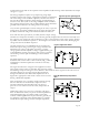
After metallization, a wide variety of possible processing steps are followed to produce a packaged
sensor. Generally, the piezo film is laminated in a protective carrier film, die cut to size, and packaged
with lead wires or crimp connectors and, often, signal conditioning electronics. The wide range of
packaged sensors, from a few square millimeters (including an ASIC chip) as a shipping damage sensor,
to multiple square meter sensors for sports scoring targets suggests the versatility of this technology.
APPLICATIONS
The sensor applications described below represent a good cross-section of the products now using
piezo film sensors.
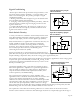
Switches
The reliability of contact switches is reduced due to contaminates like moisture and dust which foul the
contact points. Piezo film offers exceptional reliability as it is a monolithic structure, not susceptible to
this and other conventional switch failure modes. One of the most challenging of all switch
applications is found in pinball machines.
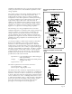
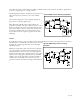
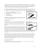
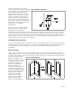
A pinball machine manufacturer uses a piezo film switch manufactured by MSI as a replacement for
the momentary rollover type switch. The switch is constructed from a laminated piezo film on a spring
steel beam, mounted as a cantilever to the end of a circuit board.