
User Manual

Page 41
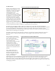
Figure 46. Layout for guarding inputs
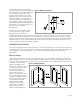
Figure 47. Signal level detector
Figure 48. Differential Op Amp interface
circuit
transferred from the film to the capacitor in the amplifier's feedback loop, which determines the output
voltage: V = Q/C
f
.
The charge amplifier requires an op amp having a high input
resistance and low bias current. A high input resistance avoids bleed-
off of the charge on the feedback capacitor, and low bias current
prevents the feedback capacitor from charging and discharging at
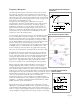
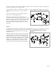
excessive rates. The layout of the charge amplifier circuit is critical.
The op-amp casing must be well grounded and the inputs should be
guarded and connected to the same ground as the casing.
A layout with guarded inputs is shown in Figure 46. Also, to prevent
leakage noise from being amplified by the op-amp, the input cable
should be terminated using a well-insulated stand-off connector.
Even with the above precautions, it is likely that the output voltage
will drift. To compensate for drift, a reset switch is generally designed into the circuit to manually reset
the output to zero at intervals. One technique is to place a reed switch in series with a resistor, which is
in parallel with the feedback capacitor C
f
. Activating the reed switch closes the switch, discharging the
voltage stored in the feedback capacitor.
Another method is to use a MOSFET device in which the
maximum output voltage and off-gate voltage determine the
minimum gate voltage of the FET. In practice, a supply
voltage greater than the amplifier voltage is applied to the gate
of the MOSFET, thereby lowering its drain/source resistance
and creating a current path for discharge of the feedback
capacitor.
The third alternative is to place a bleed resistor across the
feedback. This resistor creates a time constant (C
f
R
f
), which is
independent of the film capacitance and can be accurately
controlled.
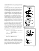
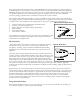
The signal level detector of Figure 47 fits applications where
large signal-to-noise ratios are desirable. This circuit is perfect
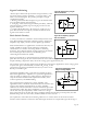
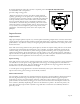
for detecting an impact among low-level vibrations. For situations where signal to noise ratios are low
and where impacts or pressures must be discerned from
background vibration, the differential amplifier circuit of
Figure 48 is appropriate. This circuit consists of two sensors
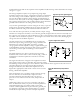
driving a differential amplifier.
This configuration uses a common-mode rejection concept.
The two switches are mechanically coupled to cancel
unwanted vibrations that stimulate both. An input or
pressure on one switch but not the other, will produce an
output.
CMOS logic offers a low-cost way to interface with piezo
film. As mentioned earlier, low-power circuits implemented
with CMOS technology are ideally suited to piezo film
switches. CMOS applications for piezo film are generally for
low frequency operation. Other characteristics to consider
include device input leakage current and input impedance,