
User Manual

Page 40
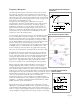
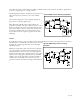
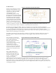
Figure 43. High frequency, low gain
FET circuit interface
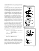
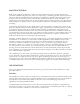
Figure 44. Low frequency, high gain
FET circuit interface
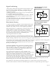
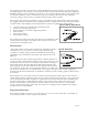
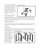
Figure 45. Op Amp Interface circuit
acting as a charge amplifier
Signal Conditioning
Because piezo film is both piezoelectric and pyroelectric, some
provision must be made to eliminate—or at least reduce—the
effect of unwanted signals. The primary principles of signal
conditioning include:
• Filtering—Electrical filters designed to give the desired band-
pass and band-rejection characteristics.
• Averaging—If the desired signal exhibits periodicity, while the
undesired signal is random, signal averaging can increase the
signal-to-noise ratio.
• Common Mode Rejection—By wiring two equal areas of a
piezo film electrode out-of-phase, unwanted common-mode
signals can be made to cancel.
Basic Switch Circuitry
A variety of circuits are available to electronically interface with
piezo film including field effect transistors (FETs), operational
amplifiers (Op Amps), and low-current digital logic (CMOS).
FETs lend themselves to applications of small size since they are
readily available in surface mount technology. Important
characteristics to consider when using FETs are switching
frequency, piezo film capacitance, leakage current of the FET in
the off-state, input bias resistance, and shielding from
electromagnetic interference (EMI).
Figures 43 and 44 show typical FET circuit configurations for a
piezo film switch. Figure 43, the common drain or source follower, applies well in applications where
simple buffering is important. Here, the circuit voltage gain is approximately one.
The common source circuit in Figure 44 is suitable for low frequency applications where voltage gain is
required. The gain is determined by resistances R
D
and R
S
. As the
gain increases, frequency bandwidth decreases by a factor of one
decade per 20 dB of gain.
Operational amplifiers offer a great deal of versatility for piezo
film switch applications. Adaptation to a particular application is
often as simple as making a few wiring changes. Important op
amp circuit characteristics include input bias resistance, film
switch capacitance, and EMI shielding.
The op amp circuit of Figure 45, a charge amplifier, suits
applications where a detected vibration actuates the switch. It also
works well in small signal applications. A charge amplifier
eliminates the effects of the time constants of both the piezo film
and connecting cable. The charge amplifier is a current operated
circuit with zero input impedance, which results in no voltage
being generated across the film. The charge amplifier quickly absorbs charges developed by the film.
With no charge left on its electrodes, the film exhibits no time constant.
The capacitance of the film and connecting cable have no adverse effect on the circuit's transfer
function. Thus tolerances on film size and cable length need not be exceptionally tight. The charge is