
User Manual

Page 36
Figure 34. Equivalent circuit of piezo film
Piezo film advantages including:
— moisture insensitivity (<.02% H
2
O absorption)
— low thermal conductivity
— low dielectric constant
— chemical inertness
— large detector sizes
The pyroelectric response of piezo film can also become a noise source for piezo sensor applications
at low frequencies. In piezoelectric applications where low frequency strain sensing is desired, there
are several convenient methods to “common-mode reject” the pyroelectric response. Examples
include:
! Two equal sized electrode patterns on one piezo film element; one electrode oriented parallel
to the d
31
and the other electrode pattern is perpendicular to the d
31
direction. Both develop
equal signals in response to pyro, but the electrode area parallel to the d
31
develops about 10X
the perpendicular electrode pattern. Subtracting the signals yields a pure piezo response.
! Two equal sized piezo film elements, laminated in a stacking configuration; one film has d
31
parallel to strain surface, the other has d
31
perpendicular to strain surface. As above, signals are
subtracted to isolate the piezo response from pyro.
! Several other common mode rejection techniques can be described by MSI’s applications
engineers.
For higher frequencies, where the rate of temperature change seen by the piezo film element is
slower than the strain event to be measured, frequency filters readily sort out the unwanted pyro
signal.
BASIC CIRCUIT CONCEPTS
A properly designed interface circuit plays a key role in the optimization of piezo film sensors. The
applications of piezo film span from toys to military sensors and interfacing to electronics is highly
application dependent. In many cases, piezo film can be directly connected to electronic circuits
without special interface considerations. However, for those cases where an interface circuit is
required, the following 3 steps are recommended:
1. Consider the frequency range and signal amplitude requirements over the desired dynamic
range.
2. Choose a proper load resistance to assure the low end operating frequency and to minimize
signal loss due to the loading effect.
3. Select a buffer circuit if the signal level is small. If a
high value load resistance is needed (such as 22MΩ or
higher value), a low leakage high impedance buffer
amplifier is recommended. JFET's or CMOS
operational amplifiers are commercially available for a
buffer.
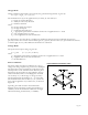
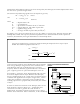
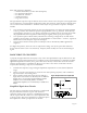
Simplified Equivalent Circuits
The first step in an interface circuit design is to understand
the piezo film characteristics as part of an electrical
equivalent circuit. Figure 34 shows a simplified equivalent
circuit of piezo film. It consists of a series capacitance with
a voltage source. The series capacitance C
f
represents piezo
film capacitance which is proportional to the film