
User Manual

Page 31
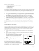
S
1
∆ l
l
d
31
(V/t) where d
31
23x10
12
m/m
V/m
∆ l d
31
(V/t) l 23x10
12
m/m
V/m
(200V)(3x10
2
m)
(9x10
6
m)
∆ l 1.53x10
5
m or 15.3 µm
∆ t td
33
(V/t) l d
33
V 33x10
12
m/m
V/m
200V 6.6x10
9
mor66a
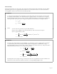
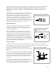
Figure 29. Piezo film bimorph
EXAMPLE 3:
A piezo film of 3 cm length (l), 2 cm width (w) and 9µm thickness (t) is subjected to an
applied voltage of V=200 volts in the 3 (thickness) direction. The amount of strain S
resulting from this electrical input is d times the applied field.
In the l direction:
In the t direction:
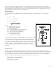
Actuators
Generally, piezo film actuator designs depend on the application requirements such as operating speed,
displacement, generated force, and available electrical power. Piezo film technology offers various design
options to meet such application requirements. Those design options include:
! Customized electrode patterns on one or both sides of the piezo film sheet.
! Multilaminate structures or bimorphs.
! Fold-over or scrolled multilayer structures.
! Extruded piezo tubes and piezo cables.
! Cast piezo polymer on various substrates
! Molded 3-D structures.
Each design option mentioned above has advantages and
disadvantages. For example, scrolled multilayer actuators
can generate a higher force but may sacrifice some
displacement.
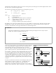
Bimorph
Like a bimetal strip, two sheets of piezo film of opposite
polarities, adhered together form a bending element, or
"bimorph" (Figure 29). An applied voltage causes one film
to lengthen, while the other contracts, causing the unit to
bend. An applied voltage of opposite polarity bends the
bimorph in the opposite direction.
The bimorph configuration converts small length changes
into sizable tip deflections, but producing low force.