
User Manual

Page 29
V
o
g
33
Xt
g
33
339x10
3
V/m
N/m
2
V
o
339x10
3
V
/
m
N/m
2
(10,000N/m
2
)(110x10
6
m)
V
0
.
373
volts
V
o
(3g
31
F
wt
(t)(g
31
)
F
w
g
31
216x10
3
V/m
N/m
2
V
o
216x10
3
V/m
N/m
2
6.45N
2.54x10
2
m
V
o
54.9volts
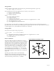
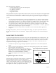
Directionality:
Piezoelectric materials are anisotropic. This means that their electrical and mechanical responses differ
depending upon the axis of applied electrical field or axis of mechanical stress or strain. Calculations
involving piezo activity must account for this directionality.
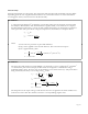
EXAMPLE 1:
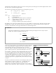
A 1.45 psi load (10,000 N/m
2
) is applied to a piezo film switch of 2.54 cm length, 2.54 cm width
and 110µm in film thickness. The switch element is rigidly backed, so the force acts to compress
the film's thickness (therefore g
33
mode). In this example the load acts on the length by width area
of the piezo film. The open circuit voltage developed across the thickness of the piezo film is:
where:
V/m is Volts out per meter of piezo film thickness
N/m
2
is stress applied to the relevant film area. The conversion from psi to
N/m
2
is approximately 7,000.
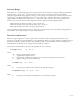
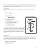
EXAMPLE 2:
The same piezo film element as in EXAMPLE 1 is subjected to a force (10,000 N/m
2
x 0.0254m
2
= 6.45 Newtons), but in this example, the film switch is configured as a membrane having a
compliant backing. Now, the force acts on the thickness cross-sectional area (wt). The piezo film is
being stretched by the load, so it is acting in the g
31
mode.
The sharp increase in output voltage results because the force is applied to the much smaller cross-
sectional area of the film. The small area results in a correspondingly higher stress.