
User Manual

Page 12
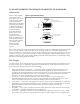
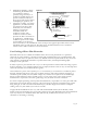
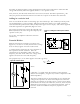
TOP ELECTRODE
BOTTOM ELECTRODE
AA
CROSS SECTION A-A
PLATED THROUGH HOLE
P.C.B
TRACE
PROTECTIVE
COAT
RIVET OR EYELET
MECHANICAL SUPPORT
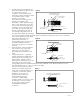
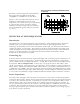
Z-AXIS CONDUCTIVE RUBBER
DT PATTERN WITH Z-AXIS CONDUCTIVE
RUBBER INTERCONNECTION
Figure 10.
! Mechanical clamping—simply
sandwiching the film between
two conductive surfaces
(possibly using a thin layer of
conductive-loaded rubber) can
provide excellent results. Two
rings can provide useful support
for diaphragms, speakers, etc.
! Capacitive Coupling - In certain
applications, no metal electrode
is required on the piezo film
itself. Thin, non-conductive
adhesives can affix the
unmetallized film to a
conductive surface. The
conductive surface in effect
provides the film’s electrodes in
ac applications. A PCB, having
conductive pads on one surface
corresponding to the desired
active sensor area, is an embodiment of this concept. The opposite piezo film surface can be
metallized with a ground electrode. The film can be sandwiched between two conductive
surfaces with or without adhesive to form electrodes.
User Etching of Piezo Film Electrodes
Patterned electrodes are available from MSI in either silver screen printed ink or as sputtered
electrodes. In some instances, customers purchase fully metallized sheets for experimentation, and
want to produce their own patterns. This is very difficult with screen printed inks as they cannot be
easily etched or mechanically braided. For sputtered electrodes, standard photolithographic
techniques work quite well.
In order to pattern piezo film in such a way as to allow penetration of film without shorting top and
bottom electrodes, a very simple technique may be employed which works on any vacuum deposited
electrodes (NOTE: not recommended for Ag Ink.)
One terminal of a power source (bench p.s.u. or 9 volt battery) is connected via a conductor pad or
block by mechanical pressure to the piece of film in question. The other terminal is brought to a
conductive point (needle, wire-end, blunt scalpel, etc.) and the area required to be isolated simply
drawn around. Sufficient current normally passes to cause arcing at the point contact and the
metallization is vaporized. Concentric "guard rings" may be drawn for extra confidence.
For more complex patterning of thin sputtered metallization, it is possible to coat the piezo film with
photoresist aerosol (both sides if necessary). The cured spray can then be exposed through a mask
using UV light, as with conventional PCB techniques, and then dipped in an etchant. Complete
etching of the very thin metal layer occurs in seconds.
Copper/Nickel metallizations etch very well with standard PCB etchant (ferric chloride). Other
metals require special etchants for good results (Aquaregia for gold). Remember that the metallization
layer may only be a few hundred atoms thick (300-700 Å), and therefore fine traces are very
vulnerable to scratching or cracking.