
User Manual

Page 8
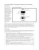
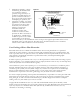
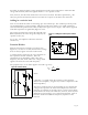
ACTIVE PIEZO FILM AREA
(TOP & BOTTOM ELECTRODES OVERLAP)
TOP ELECTRODE
ACTIVE PIEZO FILM AREA
TOP ELECTRODE
BOTTOM ELECTRODE
BOTTOM ELECTRODE
AA
CROSS SECTION A-A
AA
CROSS SECTION A-A
B
BCROSS SECTION B-B
DT PATTERN
KEYHOLE PATTERN
Figure 4. Typical piezo film patterns
LEAD ATTACHMENT TECHNIQUES FOR PIEZO FILM SENSORS
Introduction
How to make reliable
interconnection to
piezo film is one of the
most frequently asked
customer questions.
With this in mind, MSI
has paid great attention
to the development of
techniques to simplify
interconnection to
piezo film elements.
Today, most of the
sensor elements
supplied to customers
from our Division have
leads already attached.
The aim of this article
is to examine and
discuss available
interconnection
options.
Some of the most convenient interconnection techniques require that MSI apply patterned electrodes
on one or both surfaces of the piezo film—this can always be done to customers' requirements
during manufacture— alternatively, a simple method achieving the same goal is presented at the end
of the text. In general, patterned electrodes are achieved during piezo film manufacturing by screen
printing conductive inks, metal masking during sputtered electrode deposition, or chemically etching
patterns by photolithographic techniques.
The Targets
Considered here are the design objectives desired for the lead-attach method. Not all objectives can
be achieved with any one technique. Designers should identify the most important objectives and
select among the interconnection options accordingly.
! High conductivity/low resistance — surprisingly, high conductivity interconnection is not a
particularly important parameter for most piezoelectric applications. Piezo transducers are
frequently used in high-impedance circuits where inclusion of a few ohms does not usually affect
performance. More important, however, is consistence—the resistance should not fluctuate
during use since this will introduce a source of electrical noise.
! Low mass — this is especially important when the piezo film is not to be clamped to a
mechanical support structure. The acoustic effect created by the mechanical vibration of the
mass of the interconnection on an otherwise flexible structure can be dramatic.
! Low profile — many piezo film applications arise by virtue of the low thicknesses of piezo film.
Interrupting this with bulk terminations is often prohibited. Contact vibration sensors can show
distinct resonances if film is not bonded flush to the contact surface to include the
interconnection.
! Flexibility — here again is a property that must often match that of the film itself. Some degree
of flexibility is a distinct advantage in many applications.
! Low area — useful piezo devices can be quite literally be employed as "point" receivers. Small
piezo-active areas (where the top and bottom conductors fully overlap) can be configured with