Piezo Film Sensors Technical Manual Measurement Specialties, Inc. Sensor Products Division 950 Forge Avenue Norristown, PA 19403 Tel: 610.650.1500 FAX: 610.650.1509 Internet: www.msiusa.com e-mail: sensors@msiusa.
-- TABLE OF CONTENTS – Introduction . . . . . . . . . . . . . . . . . . . . . . . . . . . . . . . . . . . . . . . . . . . . . . . . . . 1 Background . . . . . . . . . . . . . . . . . . . . . . . . . . . . . . . . . . . . . . . . . . . . . . . . . . . 1 Piezoelectric Film Properties . . . . . . . . . . . . . . . . . . . . . . . . . . . . . . . . . . . . . 2 Table 1. Typical properties of piezo film . . . . . . . . . . . . . . . . . . . . . . . 3 Table 2. Comparison of piezoelectric materials . . . . . . . .
Ultrasound Applications . . . . . . . . . . . . . . . . . . . . . . . . . . . . . . . . . . . 52 Medical Imaging Ultrasound . . . . . . . . . . . . . . . . . . . . . . . . . . . 52 NonDestructive Testing (NDT) . . . . . . . . . . . . . . . . . . . . . . . . 53 Acoustic Emission . . . . . . . . . . . . . . . . . . . . . . . . . . . . . . . . . . . 53 Fluid Level Sensor . . . . . . . . . . . . . . . . . . . . . . . . . . . . . . . . . . . 53 Air Ranging Ultrasound . . . . . . . . . . . . . . . . . . . . . . .
INTRODUCTION Transducer materials convert one form of energy into another, and are widely used in sensing applications. The tremendous growth in the use of microprocessors has propelled the demand for sensors in diverse applications. Today, PIEZOELECTRIC POLYMER SENSORS are among the fastest growing of the technologies within the $18 billion worldwide sensor market.
New copolymers of PVDF, developed over the last few years, have expanded the applications of piezoelectric polymer sensors. These copolymers permit use at higher temperatures (135bC) and offer desirable new sensor shapes, like cylinders and hemispheres. Thickness extremes are possible with copolymer that cannot be readily attained with PVDF. These include ultrathin (200 Å) spin-cast coatings that enable new sensor-on-silicon applications, and cylinders with wall thicknesses in excess of 1200µm for sonar.
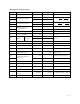
Table 1. Typical properties of piezo film Symbol t d31 d33 g31 g33 k31 Parameter Thickness Piezo Strain Constant Piezo Stress constant PVDF Copolymer 9, 28, 52, 110 <1 to 1200 23 11 -33 -38 216 162 -330 -542 12% 20% 14% 25-29% 380 for 28µm 68 for 100µm Units µm (micron, 10-6 ) 10-12 m/m C/m 2 or V/m N/m 2 10-3 V/m m/m or 2 N/m C/m 2 kt Electromechanical Coupling Factor C Capacitance Y Young’s Modulus 2-4 3-5 V0 Speed of Sound stretch: thickness: 1.5 2.3 2.2 2.
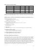
Table 2. Comparison of piezoelectric materials Property PVDF Film PZT BaTi03 10 kg/m3 1.78 7.5 5.7 Relative Permittivity ε/ε 0 12 1,200 1,700 d31 Constant -12 23 110 78 Density Units 3 (10 )C/N -3 g31 Constant (10 )Vm/N 216 10 5 k31 Constant % at 1 KHz 12 30 21 2.7 30 30 Acoustic Impedance 6 2 (10 )kg/m -sec.
Bimorph configurations (like a bimetal strip) allow the small differential displacement of two reverseconnected elements to be translated into substantial flexural motion. Small fans or optical deflectors can thus be created. Such devices consume very little real power (being capacitive in nature). Large devices may be difficult to drive due to high capacitance, especially when transformers are used to step up the drive voltage. Good amplifier design is important.
the output with pyro-generated signal. If a very long time constant is in use, then the film will generate a voltage corresponding to the change in temperature since switch-on. Since the output will be several volts per degree C, substantial offsets may be noticed. In general, however, most piezo applications will have a cut-off frequency of several Hertz or more. Connecting a device of 1nF capacitance to an oscilloscope input, even at 10 MΩ impedance, will produce a roll off below 16 Hz.
contact with the unmetallized film to collect the charge, or, capacitive coupling through thin adhesive tapes or epoxy layers can be employed for ac applications. Patterning of the electrodes is especially useful for defining specific active areas on a continuous sheet and also to allow die-cutting of elements with a clear border around the cut area.
LEAD ATTACHMENT TECHNIQUES FOR PIEZO FILM SENSORS Introduction How to make reliable interconnection to piezo film is one of the most frequently asked customer questions. With this in mind, MSI has paid great attention to the development of techniques to simplify interconnection to piezo film elements. Today, most of the sensor elements supplied to customers from our Division have leads already attached. The aim of this article is to examine and discuss available interconnection options. Figure 4.
! ! ! ! displaced or off-set lead-attach tabs. The top and bottom tabs are off-set with respect to each other (when viewed through the film thickness). This allows a precisely defined active area (overlapped electrodes) with non-piezo conductors (off-set tabs) leading to remote bonding sites, a technique most frequently employed for "small" devices.
! To affix the piezo film directly to a PCB, small "POP" or "blind" rivets Figure 5. or eyelets can be used in PLATED THROUGH HOLE conjunction with patterned film electrodes and the conductive tracks P.C.B on the PCB to allow a single PLATED THROUGH HOLE TOP ELECTRODE operation to form the interconnection.
Non-penetrative (and temporary) - Conductive-adhesive coated Copper Foil Tape (e.g., 3M #1181)—available in widths from 3mm up to 25mm. Best results are obtained by... ! ! ! ! ! ! ! Using a "reasonable" area of Figure 9. tape (perhaps about 1cm or DT PATTERN WITH COPPER TAPE more). Small pieces do tend to lift off easily. WIRE COPPER TAPE Soldering wires to the tape FIRST, then removing the liner and adhering with gentle pressure to film.
! Mechanical clamping—simply Figure 10. sandwiching the film between DT PATTERN WITH Z-AXIS CONDUCTIVE two conductive surfaces RUBBER INTERCONNECTION (possibly using a thin layer of PLATED THROUGH HOLE conductive-loaded rubber) can Z-AXIS CONDUCTIVE RUBBER TOP ELECTRODE provide excellent results. Two rings can provide useful support P.C.B for diaphragms, speakers, etc. Capacitive Coupling - In certain applications, no metal electrode is required on the piezo film BOTTOM ELECTRODE TRACE itself.
High Voltage Techniques The use of piezo film as a vibration exciter requires separate consideration. Since the impedance of a capacitive transducer decreases with frequency and approaches infinity for low frequencies, very high voltages (a few hundred volts typically) may be required to drive, for example, full audio-range loudspeakers. Frequently, transformers are used to step up moderate voltages to supply the required drive signal.
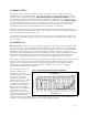
Figure 11. Dielectric permittivity and dissipation factor vs. frequency Resonance values thus depend on film thickness. They range from low MHz for thick films (1,000µ m ) to >100MHz for very thin films. Figure 11 shows the effect that frequency has on permittivity and dissipation factor at room temperature. As a result of its very low permittivity … (1 percent that of piezo ceramics), the film exhibits g-constants (voltage output coefficients) that are significantly greater than piezo ceramics (g = d/…).
PVDF has a high dielectric constant compared with most polymers, with its value being about 12 (relative to the permittivity of free space). Obviously, the capacitance of an element will increase as its plate area increases, so a large sheet of film will have a larger capacitance than a small element. Capacitance also increases as the film thickness decreases, so for the same surface geometry, a thin film will have a higher capacitance than a thick film.
this article to elaborate further on the calculations involved, but it is important to realize that this voltage will absolutely follow the applied stimulus - it is a "perfect" source. Note, however, that the node marked "X" can never be accessed! The film's capacitance C0 will always be present and connected when we monitor the "output" of the film at the electrodes. Adding in a resistive load Now we can add in the effect of connecting up to the oscilloscope.
Frequency Response This is illustrated in the following example graphs. First, a lin/lin plot is shown (Figure 15, linear yscale or amplitude, plotted against linear x-scale or frequency) with the corresponding phase plot (Figure 16) also shown in lin/lin form. Following these is a log/log plot (Figure 17), which will be dealt with in a little greater detail. Figure 15. Magnitude response of R-C filter Figure 16.
Analysis of the log/log R-C frequency response curve Some key features: # the overall characteristic of this network is known as a high-pass filter # the frequency at which the magnitude falls to 0.
Key to following figures Figure 18 shows a relatively high-frequency sine wave passing through the network. In the input spectrum, the signal is represented by a single spectral line at the appropriate frequency. This frequency is just below the filter "cut-off", and so is only slightly attenuated by the network. The resulting output wave is diminished in amplitude, and slightly shifted in phase. Figure 19 shows the same process applied to a slower sine wave.
Figure 18.
Figure 19.
Figure 20.
Figure 21.
Figure 22.
TEMPERATURE EFFECTS Many of the properties of piezo film change with excitation frequency and temperature. These properties are reversible and repeatable with either frequency or temperature cycling. Figure 23. Thermal stability of d33 constant - 70bC annealed PVDF In addition, Figure 23 shows the permanent decay of the piezoelectric strain constant d33 for PVDF, annealed at 70oC, after long term exposure to elevated temperatures.
PIEZOELECTRIC CABLE AND PROPERTIES One of the most recent developments in piezo polymer technology is piezo cable. The cable has the appearance of standard coaxial cable, but is constructed with a piezoelectric polymer insulator between the copper braid outer shield and the inner conductor (Figure 26).
Cable Typical Properties The output sensitivity of piezo cable in response to increasing impact load is shown in Figure 27a. The linearity in output for increasing force as shown in Figure 27b is typical of all piezo cable gages. PIEZOELECTRIC BASICS Figure 27a. Sensitivity vs. load Figure 27b. Piezo cable linearity Mechanical to Electrical Like water from a sponge, piezoelectric materials generate charge when squeezed.
Charge Mode: Under conditions approaching a short circuit, the generated charge density is given by: D = Q/A = d3nXn (n = 1, 2, or 3) The mechanical axis (n) of the applied stress (or strain), by convention, is: 1 = length (or stretch) direction 2 = width (or transverse) direction 3 = thickness direction where D = charge density developed Q = charge developed A = conductive electrode area d3n = appropriate piezoelectric coefficient for the axis of applied stress or strain n = axis of applied stress or strai
Directionality: Piezoelectric materials are anisotropic. This means that their electrical and mechanical responses differ depending upon the axis of applied electrical field or axis of mechanical stress or strain. Calculations involving piezo activity must account for this directionality. EXAMPLE 1: A 1.45 psi load (10,000 N/m2) is applied to a piezo film switch of 2.54 cm length, 2.54 cm width and 110µm in film thickness.
Dynamic Range Piezo film has a vast dynamic range. The sensor has been used to detect the impact of high speed particles in space having a mass of 10-12 grams, and at the other extreme, measures shock waves at 300,000 atmospheres produced during weapons testing. A recent study was conducted to determine the maximum output energy of a 52µm thick film, having an area of 155.5 mm x 18.5 mm. The film was subjected to approximately 350 MPa (in the stretch or "n = 1" direction) without failure.
EXAMPLE 3: A piezo film of 3 cm length (l), 2 cm width (w) and 9µm thickness (t) is subjected to an applied voltage of V=200 volts in the 3 (thickness) direction. The amount of strain S resulting from this electrical input is d times the applied field. In the l direction: S1 ∆l m/m d31 (V/t) where d31 23 x 10 12 l V/m ∆ l d31(V/t) l 23 x 10 12 m/m (200 V ) ( 3 x 10 2 m) V/m ( 9 x 10 6 m ) ∆ l 1.53 x 10 5 m or 15.
Thicker films and multilayers improve the force developed by the bimorph, but sacrifice displacement unless the unit can be operated at higher fields.
draw less current than parallel connections. For both parallel and series connections, the total electrical power to the actuator is identical. However, it is obvious that the lead attachment of the series connection is much simpler than that of the parallel connection for manufacturing purposes. Typical applications of the bimorph bender are cooling fans, toys, and decoratives.
Compared to mechanical or piezo ceramic actuators, multilayer Figure 32. Folded piezo film actuator piezo film actuators have fewer ringing problems due to their lower Q. Applications of multilayer actuators are micropositioners for industrial equipment, acoustic wave generators and ink jet printers. Ultrasonic Actuators Ultrasonic actuators, as discussed in this section, exclude very high frequency (> 1 MHz) transmitter applications.
The charge and voltage produced in a given film of area A permittivity ε, and thickness t is given by : Q p∆ TA V pt∆ T/ε EXAMPLE 5: A piezo film pyroelectric detector having a film thickness (t) of 9µm, a permittivity (ε) of 106x1012 C/Vm and a pyroelectric coefficient (p) of 30x10-6 C/(m2oK), undergoes a temperature increase (∆T) of 1oK due to incident IR radiation. The output voltage is given by: V (30 x 10 6 C/m 2 bK)(9 x 10 6m)(1bK) (106 x 10 12 C/Vm) V 2.
Piezo film advantages including: — moisture insensitivity (<.02% H2O absorption) — low thermal conductivity — low dielectric constant — chemical inertness — large detector sizes The pyroelectric response of piezo film can also become a noise source for piezo sensor applications at low frequencies. In piezoelectric applications where low frequency strain sensing is desired, there are several convenient methods to “common-mode reject” the pyroelectric response.
permittivity and area and inversely proportional to film thickness. The voltage source amplitude is equal to the open circuit voltage of piezo film and varies from microvolts to 100's of volts, depending on the excitation magnitude. This simplified equivalent circuit is suitable for most applications but is of limited value at very high frequencies such as that used in ultrasound transducers. Figure 35 shows an equivalent circuit as a charge generator.
Frequency Response Another important aspect of the time constant can be seen in the frequency response of the equivalent circuit. The circuit exhibits an RC high-pass filter characteristic as shown in Figure 38. In this figure, the vertical axis implies the ratio of observable output signal to the developed signal (open circuit voltage of the piezo film). Zero dB implies no loss of signal. The cutoff frequency (3 dB down) is inversely proportional to the time constant.
amplifier is determined by Q/Cf. Q is the charge developed on the piezo film and Cf is the feedback capacitance of the charge amplifier. Figure 41. Typical amplifiers for piezo film sensors The output voltage of the charge amplifier depends on the feedback capacitance, not the input capacitance. This indicates that the output voltage of a charge amplifier is independent of the cable capacitance.
Signal Conditioning Because piezo film is both piezoelectric and pyroelectric, some provision must be made to eliminate—or at least reduce—the effect of unwanted signals. The primary principles of signal conditioning include: • Filtering—Electrical filters designed to give the desired bandpass and band-rejection characteristics. • Averaging—If the desired signal exhibits periodicity, while the undesired signal is random, signal averaging can increase the signal-to-noise ratio.
transferred from the film to the capacitor in the amplifier's feedback loop, which determines the output voltage: V = Q/Cf. The charge amplifier requires an op amp having a high input resistance and low bias current. A high input resistance avoids bleedoff of the charge on the feedback capacitor, and low bias current prevents the feedback capacitor from charging and discharging at excessive rates. The layout of the charge amplifier circuit is critical.
input bias resistance, and the effect of EMI. A CMOS circuit can be used, for example, in applications to sense a single impact or a single pressure. The D-Flip Flop in Figure 49 indicates the presence of Figure 49. CMOS circuit for detecting a single impact either the impact or pressure to set off an audible alarm. The circuit in Figure 50, senses multiple impacts or pressures for counting applications. Many different CMOS circuit configurations are possible to interface with piezo film.
MANUFACTURING Rolls of piezo film are produced in a clean room environment The process begins with the melt extrusion of PVDF resin pellets into sheet form, followed by a stretching step that reduces the sheet to about one-fifth its extruded thickness. Stretching at temperatures well below the melting point of the polymer causes chain packing of the molecules into parallel crystal planes, called “beta phase”.
The "digital" piezo film switch features a simple MOSFET circuit that consumes no power during the normally-open state. In response to a direct contact force, the piezo film beam momentarily triggers the MOSFET. This provides a momentary "closure" for up to a 50 V maximum voltage. The output of this low profile contactless switch is well suited to logic-level switching. The unit does not exhibit the corrosion, pitting or bounce that are normally associated with contact switches.
In switch applications where dc response is required, piezo film Figure 53. Snap-action switch in combination with a snap dome provides a high voltage pulse. When the snap device actuates, the film is rapidly strained, typically generating a 10 volt pulse into a one megohm circuit as shown in Figure 53. This concept is especially well suited for wakeup switches, where an electronic device can be dormant for long periods without power consumption until the snap action device is actuated.
Traffic Sensors Figure 54. Permanent In-The-Road Traffic Sensor The U.S. Government is actively studying "smart highways" as an alternative to major new highway construction. The idea is that existing highways can accommodate greater vehicle densities if electronically managed.
"New Jersey barriers", the modern concrete barriers that separate opposing Figure 56. Multidirectional Sensor lanes on highways, introduce problems for multilane sensing of four lane highways. Piezo cable can solve this problem with a single sensor that has opposite polarities corresponding to each lane. Vehicles crossing the near lane produce a signal of opposite sign from vehicles in the far lane (Figure 56). This ability to provide lane activity in a single sensor is a significant development.
Machine Monitoring The fidelity of a shielded piezo film sensor in musical instruments led to the development of vibration sensors for machines. In its simplest mode, piezo film vibration sensors behave essentially like dynamic strain gages. The film does not require an external power source, yet typically generates signals greater than strain gages after amplification.
Vending Sensors Shielded dynamic strain gages of piezo film are affixed to the underside of a vending product delivery tray to verify that product was properly vended. The absence of the impact induced vibration triggers an "Out of Order" warning. In a second application, slot machine coin counting is provided by a piezo film element. The sensors confirm delivery of coins won, discouraging gamblers from falsely claiming equipment defects.
Table 6. Accelerometer Family Production Qualified Accelerometers ACH-01-XX Key Features -Wide Frequency Range -Wide Dynamic Range -High Sensitivity -Low Noise -JFET Buffer ACH-04-08-05 ACH-04-08-09 -Low Frequency Operation -Low Frequency Operation -3 Simultaneous Analog -Low Current Operation Outputs - JFET Buffer -Low current generation - JFET Buffer X-Axis --- X -- Y-Axis --- X X Z-Axis X X -- 10 mV/g 1.8 mV/g 6mV/g 1.0 Hz-20 kHz 0.5 Hz to 4 kHz 0.
Table 7.
ULTRASOUND APPLICATIONS The wide frequency response and physical attributes of its polymeric construction makes piezo film a material of choice in certain medical probes and in nondestructive testing applications. Additionally, the film sensors are found in applications in ultrasonic based sensing devices, like air-ranging ultrasound for distance measurement, in fluid level sensors, and in-flow measurement instruments using doppler shift of sound velocity perturbations which are proportional to fluid flow.
NonDestructive Testing (NDT) Advanced composite materials are very desirable as structural members. Light weight, high strength, corrosion resistance, and non-magnetic are among the advantages for these materials. The need for very routine nondestructive testing of such structures to prevent catastrophic failure due to delamination, is one of technology's greatest concerns.
The presence of fluid couples the transmit signal to the receiver to a much greater extent (60dB) than when the ultrasound energy is coupled by the air above the fluid. The excitation signal for the transmitter is a 1.1 MHz sine wave tone burst with an amplitude of 20 volts peak to peak. The required circuitry consists of a high frequency oscillator and clock, an array of analog switches, a single receiver amplifier with input gate, and a threshold detector.
elements can also be used for scanning of objects without physically moving the transducer. Each element within the transducer can be activated sequentially, as with ultrasonic arrays. AUDIO Speakers One of the earliest applications for piezo film was in stereo Figure 64. Audio speaker tweeters (Figure 64) and headset speakers developed by Pioneer Electronics.
environmental stability is critical. Waterproof microphones are being supplied for divers, withstanding total immersion in salt water without damage. SONAR Piezo ceramic materials have been used in hydrophones for Figure 65. Hydrophone SONAR since the 1940's. Ceramics have many desirable features as hydrophones including high hydrostatic sensitivity, high capacitance, ability to fabricate into shapes, and availability in thick cross-section (sensitivity is proportional to piezo element thickness).
shifted signal. Wide coverage of piezo film, with distributed electrode patterns, can be used to create individual sensor/actuator pairs. Critical damping has been achieved with this piezo film laminate by researchers at Massachusetts Institute of Technology and elsewhere. The applications for this technology include the reduction in harmful vibrations in space-based structures, fuselage for aircraft to cancel engine noise, quiet cars, quiet appliances, and a wide range of other possibilities.
Appendix A – Applications of Piezo Film APPLICATIONS OF PIEZO FILM COMPUTER INPUT/OUTPUT Physical Security & Energy Management Glass Break Detectors Keypad arrays Floor/Mat Sensor Digitizer Penetration Detection Air Mouse Contact Microphone Joystick Piezo Cable Perimeter Protection Pen (Signature verification; Handwriting Recognition) Pyrometer/Flame Sensor Printers Flow/Level Impact Flight Time Vortex Ink Drop Generation and Detection Fluidic Oscillator Toner and Ink Jet Level Air Flow Toner Activation Do
MEDICAL CONSUMER Diagnostics Apnea Monitor Ambulatory/Gait Monitors Blood Pressure Cuff Pulse Counter Stethoscope Sleep Disorder Monitors Respiratory Air Flow Isokinetics Patient Bed Monitor Ultrasound Near Field Imaging Prostate Transdermal Transluminal Coronary Arterial Breast Lithotripter Hydrophone Calibration Probes Handicapped Aides Switches Braille Reader Hearing Aid Speech Intensification Implantables Pacemaker Activity Monitor Implantable Switch Vascular Graft Monitor Micropower Source Instrument
Appendix B - INDEX OF PIEZO FILM ARTICLES [NOTE: THIS LIST IS ONLY A REFERENCE. COPIES OF THESE ARTICLES ARE NOT SUPPLIED BY MSI, INC.] CODE AUTHOR AND REFERENCE TITLE DEFOULING DF1 U.S Patent, 4,170,185 P.V. Murphy, M.J. Latour, Lectret S.A. (Switzerland) Oct. 9 1979. Preventing Marine Fouling. DF2 US DOD, Small Bus. Innovation Research Program; Ocean Piezoelectric Copolymer Antifouling Power Technologies, Inc. Topic #DARPA 90-111 System ACTUATORS (Electromotional Devices) EM1 M. Toda & S.
EM23 Minoru Toda, Ferroelectrics, 1979, Vol.22, pp 911-918 Theory of Air Flow Generation By A Resonant Type PVF2 Bimorph Cantilever Vibrator. FORCE TRANSDUCERS F1 G.R. Crane (Bell Labs, Holmdel) Transactions on Sonics and Ultrasonics. SU-25(6). November, 1978. Poly(vinylidene)Fluoride Used for Piezoelectric Coin Sensors. F4 D.S. Leitner (Columbia U.) & M.C. Rosenberger (N.Y. Psych. Inst) Behaviour Research Methods and Instrumentation. 15(5). 1983.
F42 D. A. Dillard, G. L. Anderson, D. D. Davis; 35th Sagamore Army Matls Res. Conf., Manchester, NJ June 26-30, 1988. A Preliminary Study of the use of Kynar Piezoelectric Film to Measure Peel Stresses in Adhesive Joints F43 Randy Fromm, RePlay Magazine, November 1991. Gottlieb's System 3 Pinball F44 W. Nitsche, M. Swoboda, P. Mirow, Berlin; Z. Flugwiss. Weltraumforsch. 15(1991) 223-226. Springer-Verlag 1991 Shock Detection by means of Piezofoils. F45 W. N. Nitsche, P. Mirow, J.
GENERAL G6 M. Toda (RCA Japan). J.Appl. Phys. 51(9), September 1980. Elastic Properties of Piezoelectric PVF2. G15 Pennwalt Corporation. Material Safety Data Sheet. Nov. 15, 1986.KYNAR Piezo Film G19 U.S. Patent, 4,633,122 P.F. Radice (Pennwalt) Dec. 30, 1986. Means for Electrically Connecting Electrodes on Different Surfaces of Piezoelectric Polymer Films. G23 N.A. Suttle, Marconi Research Centre. GEC Journal of Research, Vol.5, No.
G43 F. Bauer, St. Louis, FR; J. Simonne, Toulouse, FR; L. Audaire, Grenoble, FR. 8th IEEE Int'l Symp. on Applic. of Ferroelectrics, Greenville, SC, Aug 31- Sep 2, 1992 Ferroelectric Copolymer and IR Sensor Technology applied to Obstacle Detection G44 US Patent 5,424,716. Kyung Park Penetration Detection System G45 Joseph Dougherty. Penn State Mat’l Research Lab Report PVDF Copolymer - Piezoelectric Powder Composites. G46 Ken Turner.
H16 Clayton Spikes, Christopher Clark. Sea Technology, April 1996 Whales 95 - Revolutionizing Marine Mammal Monitoring Technology IMPACT SENSORS I1 U.S. Patent 4,904,894 Henry et al. February 1990 Hail Sensor I2 Joseph Paradiso, Craig Abler, Kai-yuh Hsiao, Matthew Reynolds The Magic Carpet: Physical Sensing for Immersive Environments KEYBOARDS K2 Patent 4,234,813 Heishaburo et al. (Toray Ind) November 18, 1980.
M11 R. Lerch & G.M. Sessler. J. Acoust. Soc. Am. 76(4) April 1980 Microphone with Rigidly Supported Piezo Polymer membranes. M15 I. Veit, Sennheiser Electronic Wedemark, Germany. Presented at 84th Convention of Audio Engrg Society, March 14, 1988 The Piezoelectric PVDF Film. Its properties and application in electroacoustic transducers. M17 Edward F. Downs, Jr. NCSC IR415-89 Independent Exploratory Development Piezoelectric Diver's Microphone Development.
MA19 Medical Electronics Buying Guide. Sept 1994 Buyers Guide and Market Analysis MA20 SBIR Research Proposal, Phase I Abstract A Bilaminate Electronic Bioinductive Wound Seal. MA21 Allen Zuckerwar, Robert Pretlow, John Stoughton, Donald Baker. IEEE Vol 40, No 9, September 1993 Development of a Piezopolymer Pressure Sensor for a Portable Fetal Heart Rate Monitor. MA22 Chris Henry. July 1988 Vascucare Respiration Air Monitor (R.A.M.) Phase II, Engineering Report. MA23 S. Chonan, Z.W.Jiang, Y.
MU13 F.S. Foster et.al. Ultrasound in Med. & Biol. 9(2) 151-164 1983. Breast Imaging with a Conical Transducer/Annular Array Hybrid Scanner. MU16 Peter A. Lewin & Mark Schafer. Drexel University, Philadelphia, PA. Piezoelectric Polymer Transducers for Ultrasound Dosimetry Application. MU17 M. Platte. A Polyvinylidene Fluoride Needle Hydrophone for Ultrasonic Applications. MU18 C.T. Lancee, J. Souquet, H. Ohigashi and N. Bom, Fifth Symposium on Echo-cardiology, Rotterdam, 1983.
NDT4 Systems & Instrumentation Ltd. Pershore, Worcs, England. Polymer Film Transducers. NDT8 Lewis F. Brown, Ph.D. Pennwalt Corp., Valley Forge, PA. Presented at ASNT 1989 Fall Conference Oct 9-13 1989. Piezoelectric Polymer Ultrasound Transducers for Nondestructive Testing. NDT9 Lewis F. Brown, Ph.D. Pennwalt Corp., Valley Forge, PA. Presented at 7th Intl Symposium on Applic.
OP5 S.A. Kokorowski (Hughes Research). J Opt. Soc. Am. 69(1) January, 1979. Analysis of Adaptive Optical Elements Made from Piezoelectric Bimorphs. OP6 R. Kashyap & P. Pantelis. Second Symposium on Optic Fibre Measurements, Oct. 13-14 1982 Measurement of Optical Fibre Absorption Loss: A Novel Technique. OP7 P. D. DeSouza, M. D. Mermelstein, Applied Optics, Dec. 1, 1982. Electric Field Detection with a Piezoelectric Polymer-jacketed Single-Mode Optical Fiber OP8 H.
P25 Microwatt Applications. Sea Cliff, New York. U.S.A. Comparisons of Pyroelectric and Piezoelectric Properties and Manufacturing of Several Detector Materials for Military and Scientific Applications. P26 Microwatt Applications. Sea Cliff, New York. U.S.A. Motion Detection Systems with Pyroelectric IR Detectors. P27 Alan P Doctor, Microwatt Applications Inc., Martin Rost, Servo Corporation. Pyroelectrics for Smart Munitions. P29 M. Hammerich and A. Olafsson, Physics Lab., HC Orsted Inst.
PW14 V. Hugo Schmidt. 1992 Ultrasonics Symposium Piezoelectric Energy Conversion in Wildmills. PW15 V. Hugo Schmidt. IEEE, 1986 Theoretical Electrical Power Output Per Unit Volume of PVF2 and Mechanical-ToElectrical Conversion Efficiency as Functions of Frequency. ROBOTICS R4 P. Dario, C. Domenici, R. Bardelli et al. Unpublished paper. Piezoelectric Polymers: New Sensor Materials for Robotic Applications. R5 P. Dario, R. Bardelli, D. de Rossie et al. Sensor Review. October, 1982.
S2 Pioneer Pioneers New High Polymer Molecular Transducer Technology Will Alter the Course of High Fidelity. S3 B.Locanthi, K. Maekawa, K. Sugano et al. (Pioneer, Japan) Unpublished paper. Development of a Loudspeaker System with Omni-Directional Horn Loaded High Polymer Tweeter. S4 S. Edelman & A.S. DeReggi (NBS) Journal of the Audio Engineering Society. 24(7) September 1976. Comments on "Electroacoustic Transducers with piezoelectric High Polymer Films. S6 Jesse Klapholz, Klapholz Technologies.
SP2 PCT. Patent No. WO 89/05174 ENCICCA, Traian, Anghel. 15 June 1989. Signalling System for Localizing in-out Ball Impacts by Ball Games SP3 U. S. Patent No. 4,824,107 Larry J. French, Bay Village, Ohio. April 25 1989. Sports Scoring Device including a Piezoelectric Transducer TR1 R.M. Tyburski. ITE Journal, August 1989. A Review of Road Sensor Technology for Monitoring Vehicle Traffic TR3 W. Cunagin, A. Grubbs Automated Acquisition of Truck Tire Pressure Data TR5 S. Majdi; W.
U22 E. Carome, K. Fesler, J. Shaw, D. Weinstein, L. Zitelli; Edward L. Ginzton Lab, Stanford Univ; 1979 Ultrasonics Symposium PVF2 Surface Wave Transducers U23 R. Wagers, Central Research Labs, TI, Dallas; 1979 Ultrasonics Symposium Saw Transduction on Silicon Substrates with PVF2 Films U24 R.G. Swartz & J.D. Plummer (Stanford). IEEE Transactions and Ultrasonics. SU-27(6) November 1980. On the Generation of High-Frequency Acoustic Energy with Polyvinylidene Fluoride. U25 F. Mattiocco, E.
VA22 C.K. Lee, IBM Research Div. Intern'l Conf. on Adv. Mechatronics, Tokyo May 21-24 1989. Theory of Laminated Piezopolymer Plates for Torsional and Bending Control. VA24 C.K. Lee, W.W.. Chiang, and T.C. O'Sullivan. Almaden Research Centre. IBM ACCESS Vol III. No.3 1989. Piezoelectric Modal Sensors and Actuators Achieving Critical Active Damping on a Cantilever Plate. VA35 J. Plump, Dr. J. Hubbard, Jr. (M.I.T.), T.
VA55 C.K. Lee. Intelligent Structural Systems VA56 Piezoelectric Laminates: Theory and Experiments for Distributed Sensors and Actuators Preliminary Piezo Film/Rail Assessment VA57 U.S. Patent. 4,869,101 Sept 26, 1989. James Dvorsky Batelle Memorial Institute Texture Softness Sensing VA59 C.K. Lee, F.C. Moon. Journal of Applied Mechanics June 1990, Vol 112 Modal Sensors/Actuators VA60 James E. Hubbard Jr, Calvin Lowe. December 1995 Charles Stark Draper Laboratory, Inc.
APPENDIX C -- APPLICATION NOTES Page 78
Piezoelectric Polymer Speakers Application Note 1242138 1 Aug 98 Rev A INTRODUCTION A loudspeaker is a transducer which transforms electrical signals into acoustic sound. Conventional speakers usually consist of a vibrating surface (called a diaphragm) and a driving units which is, in most cases, a voice coil driven by a magnetomotive force or a piezoelectric ceramic actuator. In piezoelectric polymer speakers, the active driving element and the air-pushing diaphragm are combined into a single unit.
Piezoelectric Polymer Speakers Application Note 1242138 Because of the curvature, the film surface basically moves in and out of the enclosure. The large film area effectively couples acoustic energy into the surrounding air. This speaker design has very good high frequency characteristics. The acoustic output is constant for frequencies up to 20 kHz.
Piezoelectric Polymer Speakers 120 Application Note 1242138 L=5cm W=5cm DISTANCE=1M 110 SPL (dB) 100 R=5cm R=10cm R=20cm R=30cm 90 80 70 60 100 1000 FREQUENCY (Hz) 10,000 100,000 Figure 2 In the design of a piezo polymer speaker, the curvature of the film needs to be considered along with other structural parameters. For example, for a small area speaker, especially with a short length L, a large radius makes the film close to a flat plane, resulting in a lower acoustic output.
Piezoelectric Polymer Speakers Application Note 1242138 LENGTH AND WIDTH OF SPEAKER FILMS - The acoustic output of a PVDF speaker is directly related to the length and width dimensions which are, in turn, determined by each different application. The sound pressure generated by a speaker at a certain distance is linearly proportional to the active area of PVDF film. Therefore, SPL is a logarithmic function of the PVDF film dimensions if the speaker area is rectangular.
Piezoelectric Polymer Speakers Application Note 1242138 The lead attachment area should not be on the PVDF film radiating surface because any non-uniformity in the radiating element can be a source for distortion of air cavity. Filling the enclosure with a sound absorbing materials such as fiberglass or absorbing foams will reduce resonances and improve the sound quality. The enclosure should be made as rigid as possible to reduce structural resonances.
DISCUSSION OF ULTRASONIC INK LEVEL SENSING Q: What is MSI’s concept for detecting low ink level? A: Right now, ink level in an ink-jet print cartridge can be measured using resistance (if the ink is partially conductive), or can be estimated by simply counting the number of droplets ejected. There are situations where neither approach will work – when the ink does not contain carbon, or where the cartridge is replaceable separately from the print head.
A: Difficult to say, before we optimize many of the variables, but 0.2 to 0.5 Mr. & Mrs. steps look practical right now. So 1.0, 1.5 and 2.0 Mr. & Mrs. walls would certainly work – if necessary, the imbalance in internal volume could be made up by adding or subtracting material elsewhere in the chamber. The step size could be smaller, if we push for “perfect” ultrasonic waveform and possibly higher frequency. Q: My cartridges have sponges inside. Will this affect the performance? A: We believe not.
(speed of sound x density) to the ink would be preferred. Given several choices, we would evaluate and select the most favorable. The wall thickness(es) have already been discussed, but it is also important to have the best possible parallelism at the sensing area. We appreciate that a finite draw angle is required for the moulding process, but if this can be minimized in the region of interest, then it makes our job much easier.