
Data Sheet

AL8805
Document number: DS35030 Rev. 4 - 2
3 of 16
www.diodes.com
July 2012
© Diodes Incorporated
A
L8805
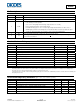
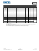
Electrical Characteristics (V
IN
= 12, @T
A
= +25°C, unless otherwise specified.)
Symbol Parameter Conditions Min Typ Max Unit
V
INSU
Internal Regulator Start Up Threshold V
IN
rising 5.9 V
V
INSH
Internal Regulator Hysteresis Threshold V
IN
falling 100 300 mV
I
Q
Quiescent Current Output not switching (Note 4) 350 µA
I
S
Input Supply Current CTRL pin floating f = 250kHz 1.8 5 mA
V
TH
Set Current Threshold Voltage 95 100 105 mV
V
TH-H
Set Threshold Hysteresis ±20 mV
I
SET
SET Pin Input Current V
SET
= V
IN
-0.1 16 22 µA
R
CTRL
CTRL Pin Input Resistance Referred to internal reference 50 kΩ
V
REF
Internal Reference Voltage 2.5 V
R
DS(on)
On Resistance of SW MOSFET I
SW
= 1A 0.25 0.4 Ω
I
SW_Leakage
Switch Leakage Current V
IN
= 30V 0.5 μA
f
OSC
Switching Frequency 1 MHz
θ
JA
Thermal Resistance Junction-to-
Ambient (Note 5)
SOT25 (Note 6) 250
°C/W
Ψ
JB
Thermal Resistance Junction-to-Lead
(Note 7)
SOT25 50
Notes: 4. AL8805 does not have a low power standby mode but current consumption is reduced when output switch is inhibited: V
SENSE
= 0V. Parameter is
tested with V
CTRL
≤ 2.5V
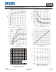
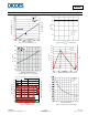
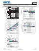
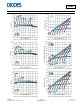
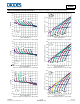
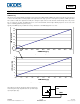
5. Refer to figure 34 for the device derating curve.
6. Test condition for SOT25: Device mounted on FR-4 PCB (25mm x 25mm 1oz copper, minimum recommended pad layout on top layer and thermal
vias to bottom layer ground plane. For better thermal performance, larger copper pad for heat-sink is needed.
7
. As SOT25 doesn’t have an exposed tab or exposed pad the majority of heat flow is though pin 2 down to ground.