
Product Specifications


CY8C29466/CY8C29566
CY8C29666/CY8C29866
Document Number: 38-12013 Rev. AB Page 5 of 67
Digital peripheral configurations include:
■ PWMs (8- and 16-bit)
■ PWMs with dead band (8- and 16-bit)
■ Counters (8- to 32-bit)
■ Timers (8- to 32-bit)
■ UART 8-bit with selectable parity (up to 2)
■ SPI slave and master (up to 2)
■ I
2
C slave and multi-master (one available as a system
resource)
■ CRC generator (8- to 32-bit)
■ IrDA (up to 2)
■ PRS generators (8- to 32-bit)
The digital blocks can be connected to any GPIO through a
series of global buses that can route any signal to any pin. The
buses also allow for signal multiplexing and for performing logic
operations. This configurability frees your designs from the
constraints of a fixed peripheral controller.
Digital blocks are provided in rows of four, where the number of
blocks varies by PSoC device family. This allows you the
optimum choice of system resources for your application. Family
resources are shown in the table titled “PSoC Device
Characteristics” on page 6.
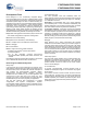
Analog System
The analog system is composed of 12 configurable blocks, each
containing an opamp circuit that allows the creation of complex
analog signal flows. Analog peripherals are very flexible and can
be customized to support specific application requirements.
Some of the more common PSoC analog functions (most
available as user modules) are:
■ ADCs (up to 4, with 6- to 14-bit resolution; selectable as
incremental, delta sigma, and SAR)
■ Filters (2-, 4-, 6-, and 8-pole band pass, low pass, and notch)
■ Amplifiers (up to 4, with selectable gain to 48x)
■ Instrumentation amplifiers (up to 2, with selectable gain to 93x)
■ Comparators (up to 4, with 16 selectable thresholds)
■ DACs (up to 4, with 6-bit to 9-bit resolution)
■ Multiplying DACs (up to 4, with 6-bit to 9-bit resolution)
■ High current output drivers (four with 30-mA drive as a core
resource)
■ 1.3-V reference (as a system resource)
■ DTMF Dialer
■ Modulators
■ Correlators
■ Peak detectors
■ Many other topologies possible
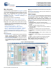
Analog blocks are provided in columns of three, which includes
one continuous time (CT) and two switched capacitor (SC)
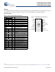
blocks, as shown in Figure 3.
Figure 3. Analog System Block Diagram
ACB00 ACB01
Bloc k Arr ay
Array Input Configuration
ACI1[1:0] ACI2[1:0]
ACB02 ACB03
ASC12 ASD13
ASD22 ASC23ASD20
ACI0[1:0] ACI3[1:0]
P0[6 ]
P0[4 ]
P0[2 ]
P0[0 ]
P2[2 ]
P2[0 ]
P2[6 ]
P2[4 ]
RefIn
AGNDIn
P0[7 ]
P0[5 ]
P0[3 ]
P0[1 ]
P2[3 ]
P2[1 ]
Re f e r e nce
Ge ne r ator s
AGNDIn
Ref In
Bandgap
Ref Hi
Ref Lo
AGND
ASD11
ASC21
ASC10
Interface to
Digital System
M8C Interface (Address Bus, Data Bus, Etc.)
Analog Reference