
Product Specifications


CY8C29466/CY8C29566
CY8C29666/CY8C29866
Document Number: 38-12013 Rev. AB Page 43 of 67
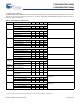
AC Digital Block Specifications
The following table lists guaranteed maximum and minimum specifications for the voltage and temperature ranges: 4.75 V to 5.25 V
and –40 °C
T
A
85 °C, or 3.0 V to 3.6 V and –40 °C T
A
85 °C, respectively. Typical parameters apply to 5 V and 3.3 V at 25 °C
and are for design guidance only.
Table 34. AC Digital Block Specifications
Function Description Min Typ Max Unit Notes
All functions Block input clock frequency
V
DD
4.75 V – – 50.4 MHz
V
DD
< 4.75 V – – 25.2 MHz
Timer Input clock frequency
No capture, V
DD
4.75 V – – 50.4 MHz
No capture, V
DD
< 4.75 V – – 25.2 MHz
With capture – – 25.2 MHz
Capture pulse width 50
[27]
––ns
Counter Input clock frequency
No enable input, V
DD
4.75 V – – 50.4 MHz
No enable input, V
DD
< 4.75 V – – 25.2 MHz
With enable input – – 25.2 MHz
Enable input pulse width 50
[27]
––ns
Dead Band Kill pulse width
Asynchronous restart mode 20 – – ns
Synchronous restart mode 50
[27]
––ns
Disable mode 50
[27]
––ns
Input clock frequency
V
DD
4.75 V – – 50.4 MHz
V
DD
< 4.75 V – – 25.2 MHz
CRCPRS
(PRS Mode)
Input clock frequency
V
DD
4.75 V – – 50.4 MHz
V
DD
< 4.75 V – – 25.2 MHz
CRCPRS
(CRC Mode)
Input clock frequency – – 25.2 MHz
SPIM Input clock frequency – – 8.2 MHz The SPI serial clock (SCLK) frequency is equal to the
input clock frequency divided by 2
SPIS Input clock (SCLK) frequency – – 4.1 MHz The input clock is the SPI SCLK in SPIS mode
Width of SS_negated between
transmissions
50
[27]
––ns
Transmitter Input clock frequency The baud rate is equal to the input clock frequency
divided by 8
V
DD
4.75 V, 2 stop bits – – 50.4 MHz
V
DD
4.75 V, 1 stop bit – – 25.2 MHz
V
DD
< 4.75 V – – 25.2 MHz
Receiver Input clock frequency The baud rate is equal to the input clock frequency
divided by 8
V
DD
4.75 V, 2 stop bits – – 50.4 MHz
V
DD
4.75 V, 1 stop bit – – 25.2 MHz
V
DD
< 4.75 V – – 25.2 MHz
Note
27. 50 ns minimum input pulse width is based on the input synchronizers running at 24 MHz (42 ns nominal period).