
Product Specifications
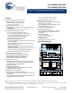
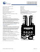


CY8C29466/CY8C29566
CY8C29666/CY8C29866
Document Number: 38-12013 Rev. AB Page 4 of 67
PSoC Functional Overview
The PSoC family consists of many Programmable
System-on-Chip controller devices. These devices are designed
to replace multiple traditional microcontroller unit (MCU)-based
system components with one, low-cost single-chip program-
mable device. PSoC devices include configurable blocks of
analog and digital logic, as well as programmable interconnects.
This architecture allows you to create customized peripheral
configurations that match the requirements of each individual
application. Additionally, a fast central processing unit (CPU),
flash program memory, SRAM data memory, and configurable
I/O are included in a range of convenient pinouts and packages.
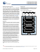
The PSoC architecture, as illustrated in the Logic Block Diagram
on page 1, consists of four main areas: PSoC core, digital
system, analog system, and system resources. Configurable
global busing allows all of the device resources to be combined
into a complete custom system. The PSoC CY8C29x66 family
can have up to five I/O ports that connect to the global digital and
analog interconnects, providing access to 8 digital blocks and
12 analog blocks.
PSoC Core
The PSoC core is a powerful engine that supports a rich feature
set. The core includes a CPU, memory, clocks, and configurable
GPIOs.
The M8C CPU core is a powerful processor with speeds up to
24 MHz, providing a 4 million instructions per second (MIPS)
8-bit Harvard-architecture microprocessor. The CPU uses an
interrupt controller with 17 vectors, to simplify programming of
real-time embedded events. Program execution is timed and
protected using the included sleep and watchdog timers (WDT).
Memory uses 32 KB of flash for program storage, 2 KB of SRAM
for data storage, and up to 2 KB of EEPROM emulated using the
flash. Program flash uses four protection levels on blocks of 64
bytes, allowing customized software information protection (IP).
The PSoC device incorporates flexible internal clock generators,
including a 24 MHz internal main oscillator (IMO) accurate to
5%
[2]
over temperature and voltage. The 24 MHz IMO can also
be doubled to 48 MHz for use by the digital system. A low-power
32 kHz internal low speed oscillator (ILO) is provided for the
sleep timer and WDT. If crystal accuracy is desired, the
32.768 kHz external crystal oscillator (ECO) is available for use
as a real-time clock (RTC) and can optionally generate a
crystal-accurate 24 MHz system clock using a PLL. The clocks,
together with programmable clock dividers (as a system
resource), provide the flexibility to integrate almost any timing
requirement into the PSoC device.
PSoC GPIOs provide connection to the CPU, and digital and
analog resources of the device. Each pin’s drive mode may be
selected from eight options, allowing great flexibility in external
interfacing. Every pin also has the capability to generate a
system interrupt on high level, low level, and change from last
read.
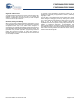
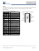
Digital System
The digital system is composed of 16 digital PSoC blocks. Each
block is an 8-bit resource that can be used alone or combined
with other blocks to form 8-, 16-, 24-, and 32-bit peripherals,
which are called user modules.
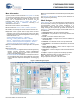
Figure 2. Digital System Block Diagram
DIGITAL SYSTEM
To System Bus
D
i
g
i
t
a
l
C
l
o
c
k
s
F
r
o
m
C
o
r
e
Digital PSoC Block Array
To Analog
System
8
Row Input
Configuration
Row Output
Configuration
88
8
Row 1
DBB10 DBB11 DCB12 DCB13
Row Input
Configuration
4
4
Row Output
Configuration
Row Input
Configuration
Row Output
Configuration
Row 2
DBB20 DBB21 DCB22 DCB23
4
4
Row 0
DBB00 DBB01 DCB02 DCB03
4
4
Row Input
Configuration
Row Output
Configuration
Row 3
DBB30 DBB31 DCB32 DCB33
4
4
GIE[7:0]
GIO[7:0]
GOE[7:0]
GOO[7:0]
Global Digital
Interconnect
Port 6
Port 7 Port 5
Port 4
Port 3
Port 2
Port 1
Port 0
Note
2. Errata: When the device is operated within 0 °C to 70 °C, the frequency tolerance is reduced to ±2.5%, but if operated at extreme temperature (below 0 °C or above
70 °C), frequency tolerance deviates from ±2.5% to ±5%. For more information, see Errata on page 61.