
Product Specifications


CY8C29466/CY8C29566
CY8C29666/CY8C29866
Document Number: 38-12013 Rev. AB Page 39 of 67
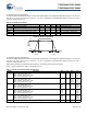
Figure 13. PLL Lock Timing Diagram
Figure 14. PLL Lock for Low Gain Setting Timing Diagram
Figure 15. External Crystal Oscillator Startup Timing Diagram
SR
POWER_UP
Power supply slew rate – – 250 V/ms V
DD
slew rate during power-up
T
POWERUP
[25]
Time from end of POR to CPU
executing code
– 16 100 ms Power-up from 0 V. See the System Resets
section of the PSoC Technical Reference
Manual
tjit_IMO
[26]
24 MHz IMO cycle-to-cycle jitter
(RMS)
– 200 700 ps N = 32
24 MHz IMO long term N
cycle-to-cycle jitter (RMS)
– 300 900
24 MHz IMO period jitter (RMS) – 100 400
tjit_PLL
[26]
24 MHz IMO cycle-to-cycle jitter
(RMS)
– 200 800 ps N = 32
24 MHz IMO long term N
cycle-to-cycle jitter (RMS)
– 300 1200
24 MHz IMO period jitter (RMS) – 100 700
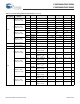
Table 29. AC Chip-Level Specifications (continued)
Symbol Description Min Typ Max Units Notes
24 MHz
F
PLL
PLL
Enable
T
PLLSLEW
PLL
Gain
0
24 MHz
F
PLL
PLL
Enable
T
PLLSLEWLOW
PLL
Gain
1
32 kHz
F
32K2
32K
Select
T
OS
Notes
25. Errata: When V
DD
of the device is pulled below ground just before power-on; the first read from each 8K Flash bank may be corrupted apart from Flash bank 0. This
can be solved by doing a dummy read from each Flash bank prior to use of the Flash banks. For more information, see Errata on page 61.
26. Refer to Cypress Jitter Specifications application note, Understanding Datasheet Jitter Specifications for Cypress Timing Products – AN5054 for more information.