
Product Specifications


CY8C29466/CY8C29566
CY8C29666/CY8C29866
Document Number: 38-12013 Rev. AB Page 37 of 67
DC Programming Specifications
The following table lists guaranteed maximum and minimum specifications for the voltage and temperature ranges: 4.75 V to 5.25 V
and –40 °C
T
A
85 °C, or 3.0 V to 3.6 V and –40 °C
T
A
85 °C, respectively. Typical parameters apply to 5 V and 3.3 V at 25 °C
and are for design guidance only.
DC I
2
C Specifications
The following table lists guaranteed maximum and minimum specifications for the voltage and temperature ranges: 4.75 V to 5.25 V
and –40 °C T
A
85 °C, or 3.0 V to 3.6 V and –40 °C T
A
85 °C, respectively. Typical parameters apply to 5 V and 3.3 V at 25 °C
and are for design guidance only.
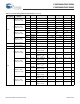
Table 27. DC Programming Specifications
Symbol Description Min Typ Max Units Notes
V
DDP
V
DD
for programming and erase
4.5 5 5.5 V
This specification applies
to the functional
requirements of external
programmer tools.
V
DDLV
Low V
DD
for verify
33.13.2 V
This specification applies
to the functional
requirements of external
programmer tools.
V
DDHV
High V
DD
for verify
5.1 5.2 5.3 V
This specification applies
to the functional
requirements of external
programmer tools.
V
DDIWRITE
Supply voltage for flash write operation
3.15 5.25 V
This specification applies
to this device when it is
executing internal flash
writes.
I
DDP
Supply current during programming or verify – 10 30 mA
V
ILP
Input low voltage during programming or verify – – 0.8 V
V
IHP
Input high voltage during programming or verify 2.2 – – V
I
ILP
Input current when applying Vilp to P1[0] or P1[1]
during programming or verify
– – 0.2 mA Driving internal pull-down
resistor
I
IHP
Input current when applying Vihp to P1[0] or P1[1]
during programming or verify
– – 1.5 mA Driving internal pull-down
resistor
V
OLV
Output low voltage during programming or verify – – V
SS
+ 0.75 V
V
OHV
Output high voltage during programming or verify V
DD
– 1.0 – V
DD
V
Flash
ENPB
Flash endurance (per block) 50,000
[18]
– – – Erase/write cycles per
block
Flash
ENT
Flash endurance (total)
[19]
1,800,000 – – – Erase/write cycles
Flash
DR
Flash data retention 10 – – Years
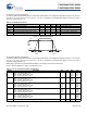
Table 28. DC I
2
C Specifications
Parameter Description Min Typ Max Units Notes
V
ILI2C
[20]
Input low level – – 0.3 × V
DD
V 3.0 V V
DD
3.6 V
– – 0.25 × V
DD
V4.75 V V
DD
5.25 V
V
IHI2C
[20]
Input high level 0.7 × V
DD
– – V 3.0 V V
DD
5.25 V
V
OLI2C
Output low level – – 0.4 V at sink current of 3 mA
– – 0.6 V at sink current of 6 mA
Notes
18. The 50,000 cycle flash endurance per block is only guaranteed if the flash is operating within one voltage range. Voltage ranges are 3.0 V to 3.6 V and 4.75 V to 5.25 V.
19. A maximum of 36 × 50,000 block endurance cycles is allowed. This may be balanced between operations on 36 × 1 blocks of 50,000 maximum cycles each,
36 × 2 blocks of 25,000 maximum cycles each, or 36 × 4 blocks of 12,500 maximum cycles each (to limit the total number of cycles to 36 × 50,000 and that no
single block ever sees more than 50,000 cycles).
For the full industrial range, the user must employ a temperature sensor user module (FlashTemp) and feed the result to the temperature argument before writing.
Refer to the Flash APIs application note Design Aids – Reading and Writing PSoC
®
Flash – AN2015 for more information.
20. All GPIOs meet the DC GPIO V
IL
and V
IH
specifications found in the DC GPIO specifications sections.The I
2
C GPIO pins also meet the mentioned specs.