
Product Specifications


CY8C29466/CY8C29566
CY8C29666/CY8C29866
Document Number: 38-12013 Rev. AB Page 28 of 67
DC Switch Mode Pump Specifications
Tab le 20 lists guaranteed maximum and minimum specifications for the voltage and temperature ranges: 4.75 V to 5.25 V and
–40 °C T
A
85 °C, or 3.0 V to 3.6 V and –40 °C T
A
85 °C, respectively. Typical parameters apply to 5 V and 3.3 V at 25 °C and
are for design guidance only.
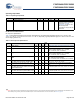
Table 20. DC Switch Mode Pump (SMP) Specifications
Symbol Description Min Typ Max Unit Notes
V
PUMP
5 V 5 V output voltage at V
DD
from
pump
4.75 5.0 5.25 V Configured as in Note 15. Average,
neglecting ripple. SMP trip voltage
is set to 5.0 V
V
PUMP
3 V 3 V output voltage at V
DD
from
pump
3.00 3.25 3.60 V Configured as in Note 15. Average,
neglecting ripple. SMP trip voltage
is set to 3.25 V
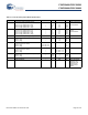
I
PUMP
Available output current
V
BAT
= 1.5 V, V
PUMP
= 3.25 V
V
BAT
= 1.8 V, V
PUMP
= 5.0 V
8
5
–
–
–
–
mA
mA
Configured as in Note 15
SMP trip voltage is set to 3.25 V
SMP trip voltage is set to 5.0 V
V
BAT
5 V Input voltage range from battery 1.8 – 5.0 V Configured as in Note 15. SMP trip
voltage is set to 5.0 V
V
BAT
3 V Input voltage range from battery 1.0 – 3.3 V Configured as in Note 15. SMP trip
voltage is set to 3.25 V
V
BATSTART
Minimum input voltage from battery
to start pump
1.2 – – V Configured as in Note 15.0 °C T
A
100. 1.25 V at T
A
= –40 °C
V
PUMP_Line
Line regulation (over V
BAT
range) – 5 – %V
O
Configured as in Note 15.
V
O
is the
“V
DD
Value for PUMP Trip” specified
by the VM[2:0] setting in the DC
POR and LVD Specification,
Table 26, “DC POR, SMP, and LVD
Specifications,” on page 36
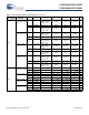
V
PUMP_Load
Load regulation – 5 – %V
O
Configured as in Note 15.
V
O
is the
“V
DD
Value for PUMP Trip” specified
by the VM[2:0] setting in Table 26,
“DC POR, SMP, and LVD Specifica-
tions,” on page 36
V
PUMP_Ripple
Output voltage ripple (depends on
capacitor/load)
– 100 – mVpp Configured as in Note 15.
Load is
5 mA
E
3
Efficiency 35 50 – % Configured as in Note 15.
Load is
5 mA. SMP trip voltage is set to
3.25 V
F
PUMP
Switching frequency – 1.4 – MHz
DC
PUMP
Switching duty cycle – 50 – %
Note
15. L
1
= 2 µH inductor, C
1
= 10 µF capacitor, D
1
= Schottky diode. See Figure 12.