
Product Specifications


CY8C29466/CY8C29566
CY8C29666/CY8C29866
Document Number: 38-12013 Rev. AB Page 26 of 67
DC Analog Output Buffer Specifications
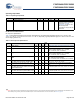
Tab le 18 and Table 19 list guaranteed maximum and minimum specifications for the voltage and temperature ranges: 4.75 V to
5.25 V and –40 °C T
A
85 °C, or 3.0 V to 3.6 V and –40 °C T
A
85 °C, respectively. Typical parameters apply to 5 V and 3.3 V
at 25 °C and are for design guidance only.
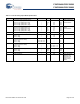
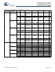
Table 18. 5-V DC Analog Output Buffer Specifications
Symbol Description Min Typ Max Unit Notes
V
OSOB
Input offset voltage (absolute value)
Power = Low, Opamp bias = Low
Power = Low, Opamp bias = High
Power = High, Opamp bias = Low
Power = High, Opamp bias = High
–
–
–
–
3.2
3.2
3.2
3.2
18
18
18
18
mV
mV
mV
mV
TCV
OSOB
Average input offset voltage drift – 5.5 26 µV/°C
V
CMOB
Common-mode input voltage range 0.5 – V
DD
– 1.0 V
R
OUTOB
Output resistance
Power = Low
Power = High
–
–
–
–
1
1
V
OHIGHOB
High output voltage swing
(Load = 32 ohms to V
DD
/2)
Power = Low
Power = High
0.5 × V
DD
+ 1.3
0.5 × V
DD
+ 1.3
–
–
–
–
V
V
V
OLOWOB
Low output voltage swing
(Load = 32 ohms to V
DD
/2)
Power = Low
Power = High
–
–
–
–
0.5 × V
DD
– 1.3
0.5 × V
DD
– 1.3
V
V
I
SOB
Supply current including bias cell (no load)
Power = Low
Power = High
–
–
1.1
2.6
2
5
mA
mA
PSRR
OB
Supply voltage rejection ratio 40 64 dB
C
L
Load capacitance – – 200 pF This specification
applies to the
external circuit
driven by the analog
output buffer.